WEO012832M-CTP model is a 0.91" COG Graphic OLED display with In-Cell Capacitive Touch Panel, which is made of resolution 128x32 pixels. This module is built-in with SSD7317 TDDI IC (Touch with Display Driver IC); it supports 4-Wire SPI and I2C interface. This SSD7317 IC is a Touch and Display Driver Integration IC (TDDI IC), which integrates touch and display microelectronics into a single chip for use on PMOLED panels, targeting applications including wearables, smart home appliances, and smart healthcare devices.
WEO012832M-CTP model adopted In-Cell Touch Panel technology, which supports SPI and I2C interface featuring four touch keys (areas) and one direction slide (supports right or left direction). The supply voltage for logic (VDD) is from 1.65V to 3.5V, typical value 3.3V, 1/32 driving duty, the display with 50% Checkboard current is 4mA @8.5V VCC (typical value), driving duty 1/32. This module can be operating at temperatures from -40℃ to +80℃; its storage temperatures range from -40℃ to +85℃.
Touch Note: Due to the high sensitivity of in-cell touch technology, proper mechanical fixation and insulation from nearby conductive components are recommended to ensure stable touch performance.
The WEO012832M-CTP model OLED module features a high contrast ratio of 10,000:1, allowing for more vibrant and deeper blacks, and brighter whites. This results in enhanced image quality, sharper details, and improved readability.
DRAWING
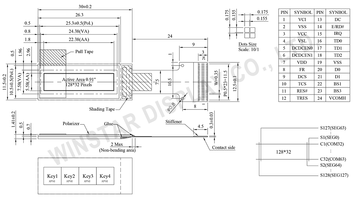
Data source ref: WEO012832MWAP3J00000
SPECIFICATIONS
Mechanical Data
Item
Dimension
Unit
Dot Matrix
128 × 32 Dots
-
Module dimension
30.0 × 11.5 × 1.41
mm
Active Area
22.38 × 5.58
mm
Pixel Size
0.155 × 0.155
mm
Pixel Pitch
0.175 × 0.175
mm
Display Mode
Passive Matrix
Display Color
Monochrome
Drive Duty
1/32 Duty
IC
SSD7317
OLED Interface
4-wire SPI,I2C
CTP Interface
SPI,I2C
Gesture
4-key single tap & slide
(Optional:Double Tap/Hold)
Size
0.91 inch
Note:Supporting more gestures may increase the response time.
Absolute Maximum Ratings
Parameter
Symbol
Min
Max
Unit
Supply Voltage for Logic
VDD
0
4.0
V
Supply Voltage for Logic
VCI
0
4.0
V
Supply Voltage for Display
VCC
0
19
V
Operating Temperature
TOP
-40
+80
°C
Storage Temperature
TSTG
-40
+85
°C
Electrical Characteristics
DC Electrical Characteristics
Item
Symbol
Condition
Min
Typ
Max
Unit
Supply Voltage for Logic
VDD
-
1.65
3.3
3.5
V
Touch controller Supply Voltage
VCI
-
3.0
-
3.5
V
Supply Voltage for Display
VCC
-
8.0
8.5
9.0
V
Input High Volt.
VIH
-
0.8×VDD
-
-
V
Input Low Volt.
VIL
-
-
-
0.2×VDD
V
Output High Volt.
VOH
-
0.9×VDD
-
-
V
Output Low Volt.
VOL
-
-
-
0.1×VDD
V
Display 50% Pixel on
ICC
VCC =8.5V
-
4
8
mA
Interface Pin Function
No.
Symbol
Function
1
VCI
Power supply pin for touch analog driving. VCI must be greater than or equal to VDD.
2
VSS
Ground pin.
3
VCC
Power Supply for Display. Most positive voltage. Connect to external source.
4
VSL
This is segment voltage (output low level) reference pin.
When external VSL is not used, connect externally to VSS. When external VSL is used, connect with resistor and diode to ground
5
DCDCEN0
Enable output pin for external DCDC circuit. NC if not used
6
DCDCEN1
Enable input pin for external DCDC circuit. Tie low if not used.
7
VDD
Power supply pin for core logic operation.
8
FR
This pin outputs RAM write synchronization signal.
It should be kept NC if it is not used.
9
DCS
This pin is the chip select input connecting to the MCU for display interface.
10
TCS
This pin is the chip select input connecting to the MCU for touch.
11
RES#
This pin is the reset signal input for display interface.
12
TRES
This pin is the reset signal input for touch.
13
DC
This pin is Data/Command control pin for display interface.
In I2C mode, this pin acts as SA0 for slave address selection.
14
E/RD#
In I2C mode, this pin acts as SA1 for slave address selection.
15
IRQ
Interrupt signal for touch reporting.
16
TD0
Serial Data Input/Output and clock for Touch
In SPI mode TD2 serves as SDOUT, TD1 serves as SDIN, and TD0 serves as the serial clock SCLK.
In I2C mode TD2 and TD1 should be tied together and serve as SDA and TD0 is the serial clock SCL. External pull up resistors.
17
TD1
18
TD2
19
VSS
Ground pin.
20
D0
The serial clock input for display interface.
21
D1
The serial data input for display interface.
22
BS1
BS1
BS3
Display Interface
Touch Interface
0
0
4 -SPI
SPI
0
1
4-SPI
I2C
1
0
I2C
SPI
1
1
I2C
I2C
23
BS3
24
VCOMH
COM signal deselected voltage level.
A capacitor should be connected between this pin and VSS.
By clicking "Allow All Cookies", you agree to the storing of cookies on your device to enhance site navigation, analyse site usage, and assist in our marketing and performance efforts. You can find further information this subject in our policy.