
우리는 귀하의 프라이버시를 소중히 여깁니다
"모든 쿠키 허용"을 클릭하면 사이트 탐색을 개선하고, 사이트 사용을 분석하며, 마케팅 및 성능 노력에 도움을 주기 위해 쿠키를 귀하의 장치에 저장하는 데 동의한 것으로 간주됩니다. 이 주제에 대한 추가 정보는 당사의 정책에서 확인할 수 있습니다. 개인정보 보호정책


WEO012832M-CTP 모델은 128x32 픽셀 해상도로 제작된 0.91인치 COG 그래픽 OLED 디스플레이이며 인셀 전용용량성 터치 패널이 장착되어 있습니다. 이 모듈은 SSD7317 TDDI IC(터치와 디스플레이 드라이버 IC)가 내장되어 있으며 4-Wire SPI 및 I2C 인터페이스를 지원합니다. 이 SSD7317 IC는 터치와 디스플레이 마이크로전자를 OLED 패널에 사용하기 위해 하나의 칩에 통합한 터치 및 디스플레이 드라이버 통합 IC(TDDI IC)로, 웨어러블 기기, 스마트 가전제품 및 스마트 헬스케어 장치 등의 응용 분야를 대상으로 합니다.
WEO012832M-CTP 모델은 인셀 터치 패널 기술을 채택하여, 오른쪽 또는 왼쪽 방향을 지원하는 4개의 터치 키(영역)와 1개의 슬라이드 방향을 지원하며 SPI 및 I2C 인터페이스를 지원합니다. 논리용 공급 전압(VDD)은 1.65V에서 3.5V까지이며, 전형적인 값은 3.3V이며, 1/32 주행 의무, 50% 체크보드 전류가 4mA @8.5V VCC(전형적인 값) 및 1/32 주행입니다. 이 모듈은 -40℃에서 +80℃까지의 온도에서 작동할 수 있으며, 저장 온도 범위는 -40℃에서 +85℃까지입니다.
터치 주의사항: In-cell 터치 기술은 환경 변화에 민감하므로, 안정적인 터치 성능을 위해 모듈을 견고하게 고정하고 주변의 도전성 부품과 적절한 절연을 유지할 것을 권장합니다.
WEO012832M-CTP 모델 OLED 모듈은 10,000:1의 높은 명암비를 갖추고 있어 더 생동감 있고 더 깊은 검은색과 밝은 흰색을 제공합니다. 이로 인해 이미지 품질이 향상되고 선명한 디테일 및 향상된 가독성을 제공합니다.
Data source ref: WEO012832MWAP3J00000
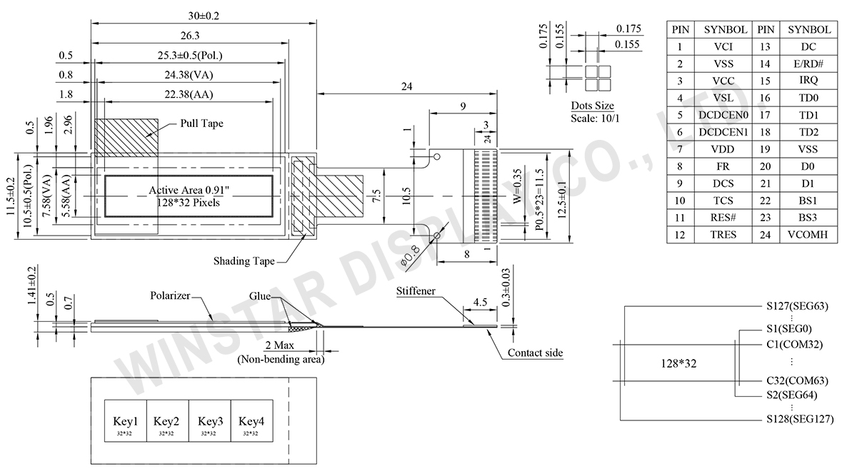
| 항목 | 치수 | 단위 |
|---|---|---|
| 도트 매트릭스 | 128 × 32 Dots | - |
| 모듈 치수 | 30.0 × 11.5 × 1.41 | mm |
| 활성 영역 | 22.38 × 5.58 | mm |
| 도트 크기 | 0.155 × 0.155 | mm |
| 도트 피치 | 0.175 × 0.175 | mm |
| 디스플레이 모드 | 패시브 매트릭스 (Passive Matrix) | |
| 디스플레이 색 | 단색 | |
| 구동 듀티 | 1/32 Duty | |
| IC | SSD7317 | |
| OLED 인터페이스 | 4-wire SPI,I2C | |
| CTP 인터페이스 | SPI,I2C | |
| 제스처 기능 | 4-Key 단일 탭 및 슬라이드 동작 (옵션: 더블 탭 / 길게 누르기) | |
| 크기 (대각선) | 0.91 인치 | |
| 매개변수 | 기호 | 최소값 | 최대값 | 단위 |
|---|---|---|---|---|
| 논리용 전원 공급 전압 | VDD | 0 | 4.0 | V |
| 논리용 전원 공급 전압 | VCI | 0 | 4.0 | V |
| 디스플레이 전원 공급 전압 | VCC | 0 | 19 | V |
| 작동 온도 | TOP | -40 | +80 | °C |
| 보관 온도 | TSTG | -40 | +85 | °C |
| 항목 | 기호 | 조건 | 최소값 | 대표값 | 최대값 | 단위 |
|---|---|---|---|---|---|---|
| 논리용 전원 공급 전압 | VDD | - | 1.65 | 3.3 | 3.5 | V |
| 터치 컨트롤러 전원 전압 | VCI | - | 3.0 | - | 3.5 | V |
| 디스플레이 전원 공급 전압 | VCC | - | 8.0 | 8.5 | 9.0 | V |
| 고전압 입력 | VIH | - | 0.8×VDD | - | - | V |
| 저전압 입력 | VIL | - | - | - | 0.2×VDD | V |
| 고전압 출력 | VOH | - | 0.9×VDD | - | - | V |
| 저전압 출력 | VOL | - | - | - | 0.1×VDD | V |
| 디스플레이 50% 픽셀 켜짐 | ICC | VCC =8.5V | - | 4 | 8 | mA |
| No. | 기호 | 기능 | ||||||||||||||||||||
|---|---|---|---|---|---|---|---|---|---|---|---|---|---|---|---|---|---|---|---|---|---|---|
| 1 | VCI | Power supply pin for touch analog driving. VCI must be greater than or equal to VDD. | ||||||||||||||||||||
| 2 | VSS | Ground pin. | ||||||||||||||||||||
| 3 | VCC | Power Supply for Display. Most positive voltage. Connect to external source. | ||||||||||||||||||||
| 4 | VSL | This is segment voltage (output low level) reference pin. When external VSL is not used, connect externally to VSS. When external VSL is used, connect with resistor and diode to ground |
||||||||||||||||||||
| 5 | DCDCEN0 | Enable output pin for external DCDC circuit. NC if not used | ||||||||||||||||||||
| 6 | DCDCEN1 | Enable input pin for external DCDC circuit. Tie low if not used. | ||||||||||||||||||||
| 7 | VDD | Power supply pin for core logic operation. | ||||||||||||||||||||
| 8 | FR | This pin outputs RAM write synchronization signal. It should be kept NC if it is not used. |
||||||||||||||||||||
| 9 | DCS | This pin is the chip select input connecting to the MCU for display interface. | ||||||||||||||||||||
| 10 | TCS | This pin is the chip select input connecting to the MCU for touch. | ||||||||||||||||||||
| 11 | RES# | This pin is the reset signal input for display interface. | ||||||||||||||||||||
| 12 | TRES | This pin is the reset signal input for touch. | ||||||||||||||||||||
| 13 | DC | This pin is Data/Command control pin for display interface. In I2C mode, this pin acts as SA0 for slave address selection. |
||||||||||||||||||||
| 14 | E/RD# | In I2C mode, this pin acts as SA1 for slave address selection. | ||||||||||||||||||||
| 15 | IRQ | Interrupt signal for touch reporting. | ||||||||||||||||||||
| 16 | TD0 | Serial Data Input/Output and clock for Touch In SPI mode TD2 serves as SDOUT, TD1 serves as SDIN, and TD0 serves as the serial clock SCLK. In I2C mode TD2 and TD1 should be tied together and serve as SDA and TD0 is the serial clock SCL. External pull up resistors. |
||||||||||||||||||||
| 17 | TD1 | |||||||||||||||||||||
| 18 | TD2 | |||||||||||||||||||||
| 19 | VSS | Ground pin. | ||||||||||||||||||||
| 20 | D0 | The serial clock input for display interface. | ||||||||||||||||||||
| 21 | D1 | The serial data input for display interface. | ||||||||||||||||||||
| 22 | BS1 |
|
||||||||||||||||||||
| 23 | BS3 | |||||||||||||||||||||
| 24 | VCOMH | COM signal deselected voltage level. A capacitor should be connected between this pin and VSS. |

"모든 쿠키 허용"을 클릭하면 사이트 탐색을 개선하고, 사이트 사용을 분석하며, 마케팅 및 성능 노력에 도움을 주기 위해 쿠키를 귀하의 장치에 저장하는 데 동의한 것으로 간주됩니다. 이 주제에 대한 추가 정보는 당사의 정책에서 확인할 수 있습니다. 개인정보 보호정책