私たちはあなたのプライバシーを大切にします
「すべてのクッキーを許可」をクリックすると、サイトのナビゲーションを向上させ、サイト使用状況を分析し、マーケティングおよびパフォーマンスの取り組みを支援するために、クッキーをデバイスに保存することに同意したことになります。この件に関する詳細情報は、ポリシーをご覧ください。プライバシーポリシー


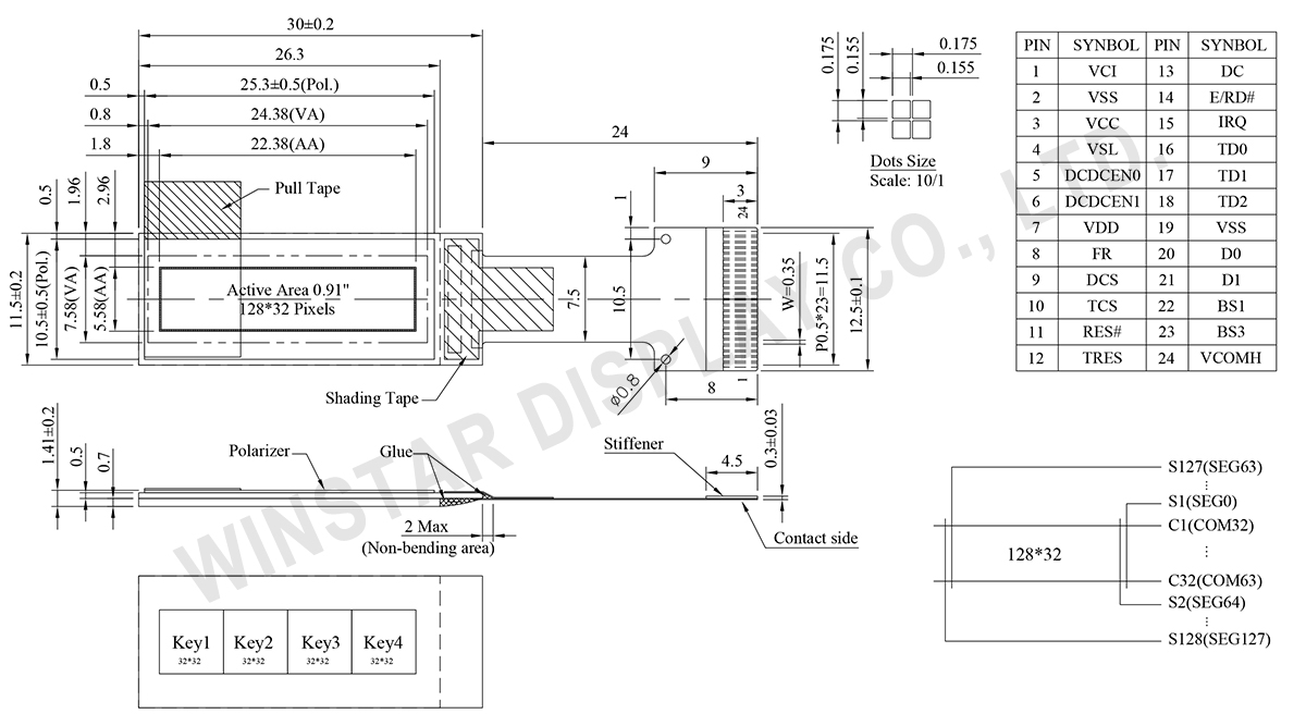
型番 WEO012832M-CTP
►タイプ: グラフィック有機ELディスプレイ
►結構: COG
►サイズ: 0.91インチ
►128 x 32 ドットマトリックス
►IC:SSD7317
►3V電源電圧
►1/32 duty
►インターフェース: SPI/I2C
►インセル型タッチパネル, In-Cell タッチパネル
►発光色: 白色 / 黄色
WEO012832M-CTPモデルは解像度128x32ピクセルで作られたセル内静電容量式In-Cellインセルタッチパネルを備えた0.91インチCOGグラフィック有機ELです。このモジュールにSSD7317 TDDI IC(Touch with Display Driver IC)が組み込まれて、4線式SPI及びI2Cインターフェースをサポートします。このSSD7317 ICはタッチアンドディスプレイドライバー統合IC(TDDI IC)で、ウェアラブル、スマート家電、スマートヘルスケアデバイス等のアプリケーションを対象として、タッチアンドディスプレイマイクロエレクトロニクスを単一チップに統合してPM有機ELパネルで使用します。
WEO012832M-CTPモデルはインセルタッチパネル技術を採用して、4つのタッチキー(領域)と1つの方向スライド(右または左方向をサポート)を備えたSPI及びI2Cインターフェースをサポートします。 ロジック(VDD)の供給電圧は1.65V〜3.5Vにして、標準値3.3Vで、1/32駆動デューティで、50%チェックボード電流のディスプレイは4mA @ 8.5V VCC(標準値)で、駆動デューティ1/32 です。このモジュールの操作温度範囲が-40℃~+80℃で、保存温度範囲が-40℃~+85℃です。
タッチに関する注意事項:In-cell タッチ技術は環境変化に対して高い感度を持つため、安定したタッチ性能を確保するには、モジュールを確実に固定し、周囲の導電部品から適切に絶縁することを推奨します。
WEO012832M-CTPモデルのOLEDモジュールは、10,000:1の高コントラスト比を特長としており、より鮮やかで深い黒、明るい白を実現します。これにより、画像品質が向上し、より鮮明なディテールと読みやすさが向上します。
Data source ref: WEO012832MWAP3J00000
| 項目 | 仕様 | 単位 |
|---|---|---|
| ドットマトリックス | 128 × 32 Dots | - |
| モジュールサイズ | 30.0 × 11.5 × 1.41 | mm |
| 有効エリア | 22.38 × 5.58 | mm |
| ドットサイズ | 0.155 × 0.155 | mm |
| ドットピッチ | 0.175 × 0.175 | mm |
| 表示モード | パッシブマトリックス | |
| 発光色 | モノクロ | |
| 駆動方法 | 1/32 Duty | |
| IC | SSD7317 | |
| OLED インターフェイス | 4-wire SPI,I2C | |
| CTP インターフェイス | SPI,I2C | |
| ジェスチャー機能 | 4キーのシングルタップおよびスライド操作(オプション:ダブルタップ/長押し) | |
| 表示サイズ | 0.91インチ | |
| パラメーター | 記号 | 最小値 | 最大値 | 単位 |
|---|---|---|---|---|
| ロジック電源電圧 | VDD | 0 | 4.0 | V |
| ロジック電源電圧 | VCI | 0 | 4.0 | V |
| ディスプレイの供給電圧 | VCC | 0 | 19 | V |
| 操作温度 | TOP | -40 | +80 | °C |
| 保存温度 | TSTG | -40 | +85 | °C |
| 項目 | 記号 | 条件 | 最小値 | 典型値 | 最大値 | 単位 |
|---|---|---|---|---|---|---|
| ロジック電源電圧 | VDD | - | 1.65 | 3.3 | 3.5 | V |
| タッチパネル コントローラー 電源電圧 | VCI | - | 3.0 | - | 3.5 | V |
| ディスプレイの供給電圧 | VCC | - | 8.0 | 8.5 | 9.0 | V |
| 高レベル入力 | VIH | - | 0.8×VDD | - | - | V |
| 低レベル入力 | VIL | - | - | - | 0.2×VDD | V |
| 高レベル出力 | VOH | - | 0.9×VDD | - | - | V |
| 低レベル出力 | VOL | - | - | - | 0.1×VDD | V |
| ディスプレイ50%ピクセル点灯 | ICC | VCC =8.5V | - | 4 | 8 | mA |
| No. | 記号 | 説明 | ||||||||||||||||||||
|---|---|---|---|---|---|---|---|---|---|---|---|---|---|---|---|---|---|---|---|---|---|---|
| 1 | VCI | Power supply pin for touch analog driving. VCI must be greater than or equal to VDD. | ||||||||||||||||||||
| 2 | VSS | Ground pin. | ||||||||||||||||||||
| 3 | VCC | Power Supply for Display. Most positive voltage. Connect to external source. | ||||||||||||||||||||
| 4 | VSL | This is segment voltage (output low level) reference pin. When external VSL is not used, connect externally to VSS. When external VSL is used, connect with resistor and diode to ground |
||||||||||||||||||||
| 5 | DCDCEN0 | Enable output pin for external DCDC circuit. NC if not used | ||||||||||||||||||||
| 6 | DCDCEN1 | Enable input pin for external DCDC circuit. Tie low if not used. | ||||||||||||||||||||
| 7 | VDD | Power supply pin for core logic operation. | ||||||||||||||||||||
| 8 | FR | This pin outputs RAM write synchronization signal. It should be kept NC if it is not used. |
||||||||||||||||||||
| 9 | DCS | This pin is the chip select input connecting to the MCU for display interface. | ||||||||||||||||||||
| 10 | TCS | This pin is the chip select input connecting to the MCU for touch. | ||||||||||||||||||||
| 11 | RES# | This pin is the reset signal input for display interface. | ||||||||||||||||||||
| 12 | TRES | This pin is the reset signal input for touch. | ||||||||||||||||||||
| 13 | DC | This pin is Data/Command control pin for display interface. In I2C mode, this pin acts as SA0 for slave address selection. |
||||||||||||||||||||
| 14 | E/RD# | In I2C mode, this pin acts as SA1 for slave address selection. | ||||||||||||||||||||
| 15 | IRQ | Interrupt signal for touch reporting. | ||||||||||||||||||||
| 16 | TD0 | Serial Data Input/Output and clock for Touch In SPI mode TD2 serves as SDOUT, TD1 serves as SDIN, and TD0 serves as the serial clock SCLK. In I2C mode TD2 and TD1 should be tied together and serve as SDA and TD0 is the serial clock SCL. External pull up resistors. |
||||||||||||||||||||
| 17 | TD1 | |||||||||||||||||||||
| 18 | TD2 | |||||||||||||||||||||
| 19 | VSS | Ground pin. | ||||||||||||||||||||
| 20 | D0 | The serial clock input for display interface. | ||||||||||||||||||||
| 21 | D1 | The serial data input for display interface. | ||||||||||||||||||||
| 22 | BS1 |
|
||||||||||||||||||||
| 23 | BS3 | |||||||||||||||||||||
| 24 | VCOMH | COM signal deselected voltage level. A capacitor should be connected between this pin and VSS. |

「すべてのクッキーを許可」をクリックすると、サイトのナビゲーションを向上させ、サイト使用状況を分析し、マーケティングおよびパフォーマンスの取り組みを支援するために、クッキーをデバイスに保存することに同意したことになります。この件に関する詳細情報は、ポリシーをご覧ください。プライバシーポリシー