Das Modell WEO012832M-CTP ist ein 0,91 Zoll COG-Grafik-OLED-Display mit In-Cell kapazitivem Touchpanel und einer Auflösung von 128x32 Pixeln. Dieses Modul ist mit dem SSD7317 TDDI-IC (Touch with Display Driver IC) ausgestattet und unterstützt die Schnittstellen 4-Wire SPI und I2C. Dieses SSD7317-IC ist ein Touch- und Display-Treiber-Integrations-IC (TDDI-IC), das Touch- und Display-Mikroelektronik in einem einzigen Chip für die Verwendung auf PMOLED-Panels integriert und auf Anwendungen abzielt, einschließlich Wearables, Smart-Home-Geräte und Smart-Healthcare-Geräte.
Das Modell WEO012832M-CTP verwendet die In-Cell-Touchpanel-Technologie, die die SPI- und I2C-Schnittstelle unterstützt und über vier Touch-Tasten (Bereiche) und eine Richtungsschiebe-Funktion (Unterstützung der rechten oder linken Richtung) verfügt. Die Versorgungsspannung für die Logik (VDD) beträgt 1,65V bis 3,5V, typischer Wert 3,3V, 1/32-Ansteuerungsduty, der Bildschirm mit 50% Checkboard-Strom beträgt 4mA @8,5V VCC (typischer Wert), 1/32-Ansteuerungsduty. Dieses Modul kann bei Temperaturen von -40°C bis +80°C betrieben werden; der Bereich der Lagertemperaturen reicht von -40°C bis +85°C.
Hinweis zur Touch-Funktion: Aufgrund der hohen Empfindlichkeit der In-Cell-Touch-Technologie wird empfohlen, das Modul mechanisch sicher zu befestigen und ausreichend von benachbarten leitfähigen Komponenten zu isolieren, um eine stabile Touch-Funktion zu gewährleisten.
Das OLED-Modell WEO012832M-CTP verfügt über ein hohes Kontrastverhältnis von 10.000:1, was lebendigere und tiefere Schwarztöne sowie hellere Weißtöne ermöglicht. Dies führt zu einer verbesserten Bildqualität, schärferen Details und verbesserter Lesbarkeit.
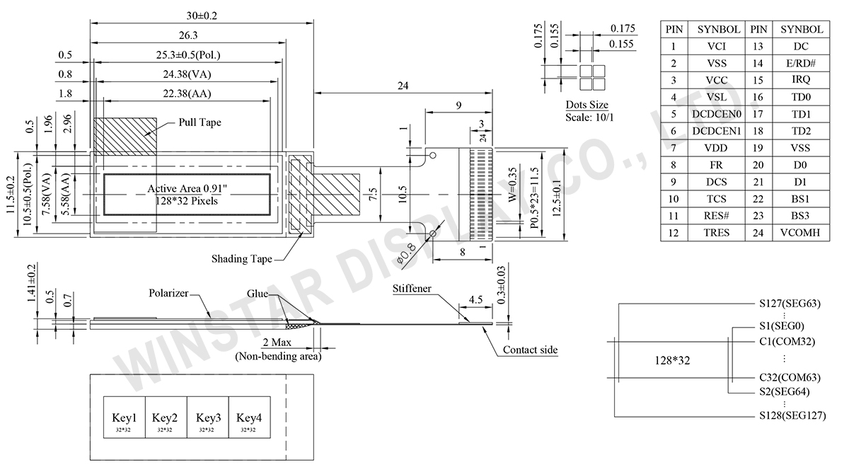
Zeichnung
Data source ref: WEO012832MWAP3J00000
Technische Daten
mechanische Daten
Artikel
Ausmaß
Einheit
Punktmatrix
128 × 32 Dots
-
Abmaße der modul
30,0 × 11,5 × 1,41
mm
Aktiver Bereich
22,38 × 5,58
mm
Punktgröße
0,155 × 0,155
mm
Punktabstand
0,175 × 0,175
mm
der Anzeigemodus
Passive Matrix
die Farbe des Displays
Moncohromes
Drive Duty
1/32 Duty
IC
SSD7317
OLED-Schnittstelle
4-wire SPI,I2C
CTP-Schnittstelle
SPI,I2C
Gestenfunktionen
4 Tasten mit einfachem Tippen und Wischbewegung (optional: Doppeltippen / langes Drücken)
Größe (Diagonale)
0,91 Zoll
Hinweis: Die Unterstützung zusätzlicher Gesten kann die Reaktionszeit erhöhen.
Absolute Grenzwerte
Parameter
Symbol
Mindestwert
Maximalwert
Einheit
Versorgungsspannung für Logik
VDD
0
4,0
V
Versorgungsspannung für Logik
VCI
0
4,0
V
Versorgungs-Spannung für das Display
VCC
0
19
V
Betriebstemperatur
TOP
-40
+80
°C
Lagertemperatur
TSTG
-40
+85
°C
elektronische Eingenschaften
DC elektronische Eingenschaften
Artikel
Symbol
Bedingung
Mindestwert
typischer Wert
Maximalwert
Einheit
Versorgungsspannung für Logik
VDD
-
1,65
3,3
3,5
V
Touch controller Supply Voltage
VCI
-
3,0
-
3,5
V
Versorgungs-Spannung für das Display
VCC
-
8,0
8,5
9,0
V
Hochpegel-Eingang
VIH
-
0,8×VDD
-
-
V
Niedrigpegel-Eingang
VIL
-
-
-
0,2×VDD
V
Hochpegel-Ausgang
VOH
-
0,9×VDD
-
-
V
Niedrigpegel-Ausgang
VOL
-
-
-
0,1×VDD
V
Display 50% Pixel an
ICC
VCC =8,5V
-
4
8
mA
Schnittstelle Pin-Funktion
No.
Symbol
Beschreibung
1
VCI
Power supply pin for touch analog driving. VCI must be greater than or equal to VDD.
2
VSS
Ground pin.
3
VCC
Power Supply for Display. Most positive voltage. Connect to external source.
4
VSL
This is segment voltage (output low level) reference pin.
When external VSL is not used, connect externally to VSS. When external VSL is used, connect with resistor and diode to ground
5
DCDCEN0
Enable output pin for external DCDC circuit. NC if not used
6
DCDCEN1
Enable input pin for external DCDC circuit. Tie low if not used.
7
VDD
Power supply pin for core logic operation.
8
FR
This pin outputs RAM write synchronization signal.
It should be kept NC if it is not used.
9
DCS
This pin is the chip select input connecting to the MCU for display interface.
10
TCS
This pin is the chip select input connecting to the MCU for touch.
11
RES#
This pin is the reset signal input for display interface.
12
TRES
This pin is the reset signal input for touch.
13
DC
This pin is Data/Command control pin for display interface.
In I2C mode, this pin acts as SA0 for slave address selection.
14
E/RD#
In I2C mode, this pin acts as SA1 for slave address selection.
15
IRQ
Interrupt signal for touch reporting.
16
TD0
Serial Data Input/Output and clock for Touch
In SPI mode TD2 serves as SDOUT, TD1 serves as SDIN, and TD0 serves as the serial clock SCLK.
In I2C mode TD2 and TD1 should be tied together and serve as SDA and TD0 is the serial clock SCL. External pull up resistors.
17
TD1
18
TD2
19
VSS
Ground pin.
20
D0
The serial clock input for display interface.
21
D1
The serial data input for display interface.
22
BS1
BS1
BS3
Display Interface
Touch Interface
0
0
4 -SPI
SPI
0
1
4-SPI
I2C
1
0
I2C
SPI
1
1
I2C
I2C
23
BS3
24
VCOMH
COM signal deselected voltage level.
A capacitor should be connected between this pin and VSS.
Durch Klicken auf „Alle Cookies zulassen“ stimmen Sie der Speicherung von Cookies auf Ihrem Gerät zu, um die Navigation auf der Website zu verbessern, die Nutzung der Website zu analysieren und unsere Marketing- und Leistungsbemühungen zu unterstützen. Weitere Informationen zu diesem Thema finden Sie in unserer Richtlinie. Datenschutzrichtlinie