


 - WEA128128G")
我們重視您的隱私
通過點擊「允許所有 Cookie」,代表您同意在您的設備上存儲 Cookie 以增強網站瀏覽體驗、分析網站使用情況並協助我們的行銷和網站效能優化工作。您可以在我們的隱私權政策中找到有關於此的更多資訊。


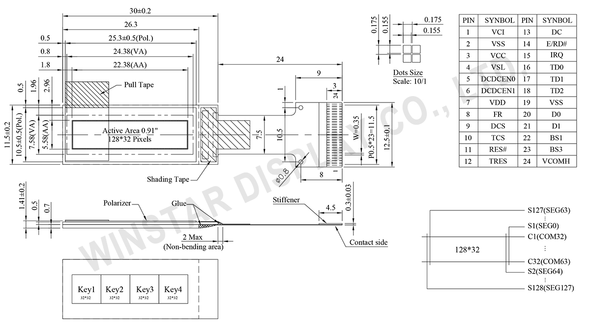
型號 WEO012832M-CTP
►類型: 繪圖型
►結構: COG
►尺寸: 0.91吋
►128 x 32 點陣
►IC:SSD7317
►3V電源電壓
►1/32 duty
►介面: SPI,I2C
►In Cell 內嵌式觸控面板
►發光顏色: 白色 / 黃色
WEO012832M-CTP型號是一款0.91吋COG繪圖型OLED顯示器,採用In-Cell內嵌式電容觸控面板,解析度為128x32像素。模組內建SSD7317 TDDI IC,此款IC採用TDDI IC為觸控與面板整合驅動IC (Touch with Display Driver),將面板驅動IC和觸控面板IC整合成一顆晶片的觸控技術,WEO012832M-CTP 型號PMOLED模組採用內嵌式 (In-Cell ) 觸控技術,主要可應用於穿戴裝置、智能家電和智能醫療保健裝置等產品應用。
WEO012832M-CTP型號採用In-Cell 內嵌式觸控面板技術,支援4線SPI和I2C介面,並支援四個區域觸控和單一方向左右滑動。邏輯電源電壓(VDD)為1.65V~3.5V,typical值3.3V,50%顯示畫面耗電流4mA @8.5V VCC (typical 值),驅動方式1/32。此模組工作溫度範圍為-40℃~+80℃;儲存溫度範圍為-40℃~+85℃。
觸控注意事項:由於 In-cell 觸控技術對環境變化相當敏感,建議在機構設計上確實固定模組,並與周圍導電元件保持適當的絕緣距離,以確保穩定的觸控效能。
WEO012832M-CTP 型號 OLED 模組具有 10,000:1 的高對比度,可呈現更鮮豔、更深的黑色以及更明亮的白色。 這樣可以提高影像品質、更清晰的細節並提高可讀性。
Data source ref: WEO012832MWAP3J00000
| 項目 | 規格說明 | 單位 |
|---|---|---|
| 點陣 | 128 × 32 Dots | - |
| 模組尺寸 | 30.0 × 11.5 × 1.41 | mm |
| 有效區域 | 22.38 × 5.58 | mm |
| 像素大小 | 0.155 × 0.155 | mm |
| 像素間距 | 0.175 × 0.175 | mm |
| 顯示模式 | 被動矩陣 | |
| 顯示顏色 | 單色 | |
| 驅動方式 | 1/32 Duty | |
| IC | SSD7317 | |
| OLED 介面 | 4線 SPI,I2C | |
| CTP 介面 | SPI,I2C | |
| 手勢 | 4-Key 單次點擊與滑動操作(可選:雙擊、長按) | |
| 尺寸 | 0.91 吋 | |
| 參數 | 符號 | 最小值 | 最大值 | 單位 |
|---|---|---|---|---|
| 邏輯電源電壓 | VDD | 0 | 4.0 | V |
| 邏輯電源電壓 | VCI | 0 | 4.0 | V |
| 顯示電源電壓 | VCC | 0 | 19 | V |
| 工作溫度 | TOP | -40 | +80 | °C |
| 儲存溫度 | TSTG | -40 | +85 | °C |
| 項目 | 符號 | 條件 | 最小值 | 典型值 | 最大值 | 單位 |
|---|---|---|---|---|---|---|
| 邏輯電源電壓 | VDD | - | 1.65 | 3.3 | 3.5 | V |
| 觸控控制器電源電壓 | VCI | - | 3.0 | - | 3.5 | V |
| 顯示電源電壓 | VCC | - | 8.0 | 8.5 | 9.0 | V |
| 輸入高準位 | VIH | - | 0.8×VDD | - | - | V |
| 輸入低準位 | VIL | - | - | - | 0.2×VDD | V |
| 輸出高準位 | VOH | - | 0.9×VDD | - | - | V |
| 輸出低準位 | VOL | - | - | - | 0.1×VDD | V |
| 顯示器 50% 像素開啟 | ICC | VCC =8.5V | - | 4 | 8 | mA |
| No. | 符號 | 功能說明 | ||||||||||||||||||||
|---|---|---|---|---|---|---|---|---|---|---|---|---|---|---|---|---|---|---|---|---|---|---|
| 1 | VCI | Power supply pin for touch analog driving. VCI must be greater than or equal to VDD. | ||||||||||||||||||||
| 2 | VSS | Ground pin. | ||||||||||||||||||||
| 3 | VCC | Power Supply for Display. Most positive voltage. Connect to external source. | ||||||||||||||||||||
| 4 | VSL | This is segment voltage (output low level) reference pin. When external VSL is not used, connect externally to VSS. When external VSL is used, connect with resistor and diode to ground |
||||||||||||||||||||
| 5 | DCDCEN0 | Enable output pin for external DCDC circuit. NC if not used | ||||||||||||||||||||
| 6 | DCDCEN1 | Enable input pin for external DCDC circuit. Tie low if not used. | ||||||||||||||||||||
| 7 | VDD | Power supply pin for core logic operation. | ||||||||||||||||||||
| 8 | FR | This pin outputs RAM write synchronization signal. It should be kept NC if it is not used. |
||||||||||||||||||||
| 9 | DCS | This pin is the chip select input connecting to the MCU for display interface. | ||||||||||||||||||||
| 10 | TCS | This pin is the chip select input connecting to the MCU for touch. | ||||||||||||||||||||
| 11 | RES# | This pin is the reset signal input for display interface. | ||||||||||||||||||||
| 12 | TRES | This pin is the reset signal input for touch. | ||||||||||||||||||||
| 13 | DC | This pin is Data/Command control pin for display interface. In I2C mode, this pin acts as SA0 for slave address selection. |
||||||||||||||||||||
| 14 | E/RD# | In I2C mode, this pin acts as SA1 for slave address selection. | ||||||||||||||||||||
| 15 | IRQ | Interrupt signal for touch reporting. | ||||||||||||||||||||
| 16 | TD0 | Serial Data Input/Output and clock for Touch In SPI mode TD2 serves as SDOUT, TD1 serves as SDIN, and TD0 serves as the serial clock SCLK. In I2C mode TD2 and TD1 should be tied together and serve as SDA and TD0 is the serial clock SCL. External pull up resistors. |
||||||||||||||||||||
| 17 | TD1 | |||||||||||||||||||||
| 18 | TD2 | |||||||||||||||||||||
| 19 | VSS | Ground pin. | ||||||||||||||||||||
| 20 | D0 | The serial clock input for display interface. | ||||||||||||||||||||
| 21 | D1 | The serial data input for display interface. | ||||||||||||||||||||
| 22 | BS1 |
|
||||||||||||||||||||
| 23 | BS3 | |||||||||||||||||||||
| 24 | VCOMH | COM signal deselected voltage level. A capacitor should be connected between this pin and VSS. |

通過點擊「允許所有 Cookie」,代表您同意在您的設備上存儲 Cookie 以增強網站瀏覽體驗、分析網站使用情況並協助我們的行銷和網站效能優化工作。您可以在我們的隱私權政策中找到有關於此的更多資訊。