
 - WEA012864A")
我們重視您的隱私
通過點擊「允許所有 Cookie」,代表您同意在您的設備上存儲 Cookie 以增強網站瀏覽體驗、分析網站使用情況並協助我們的行銷和網站效能優化工作。您可以在我們的隱私權政策中找到有關於此的更多資訊。


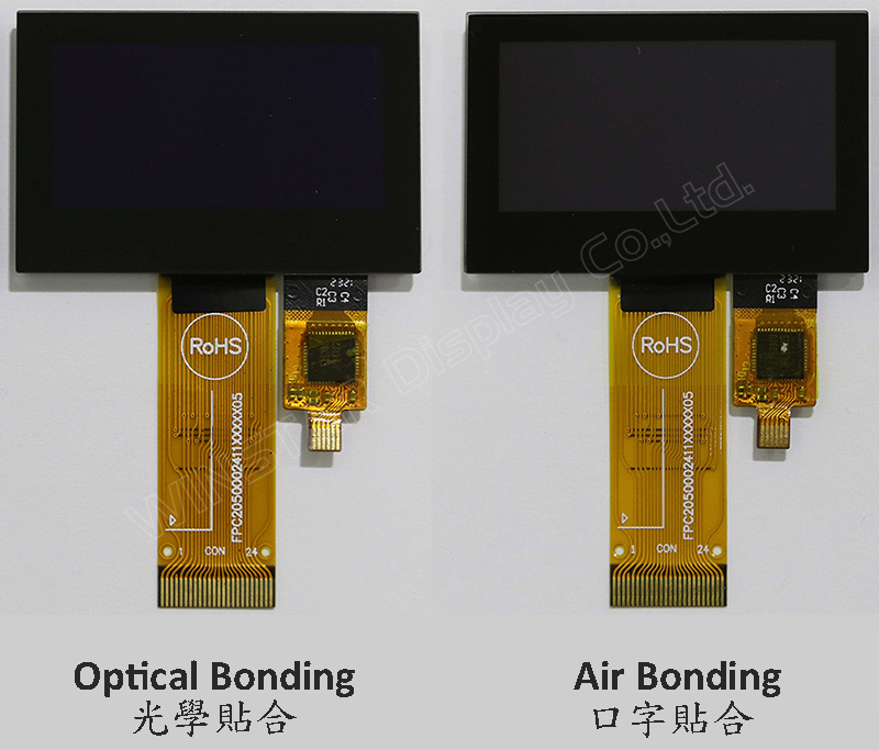
WEO012864A-CTP是一款1.54吋COG結構繪圖型OLED顯示器模組搭載CTP電容式觸控面板,解析度為128x64像素,內建SSD1309 IC,支援6800/8080 8-bit並列傳輸介面、4線SPI及I2C介面;邏輯電源電壓為 2.8V ~ 3.3V,Typical 值為3.0V,顯示器電源電壓 12.5V,驅動方式1/64。此型號提供兩種 CTP 結構選項;一種為採用口字貼合 (Air Bonding) 技術的CTP觸控面板,另一選項為採用光學貼合 (Optical Bonding) 技術的CTP觸控面板,此兩種CTP觸控面板觸控IC皆使用FT6336U,均支援I2C介面和單點觸控。
WEO012864A型號搭載CTP觸控面板非常適用於智慧家居應用、智能技術設備、儀表裝置、工業控制系統、醫療儀器…等。此模組工作溫度範圍為-10℃~+60℃;儲存溫度範圍為-20℃~+70℃。
WEO012864A-CTP型號 OLED 模組具有 10,000:1 的高對比度,可呈現更鮮豔、更深的黑色以及更明亮的白色。 這樣可以提高影像品質、更清晰的細節並提高可讀性。
| 項目 | 規格說明 | 單位 |
|---|---|---|
| 點陣(解析度) | 128 x 64 | - |
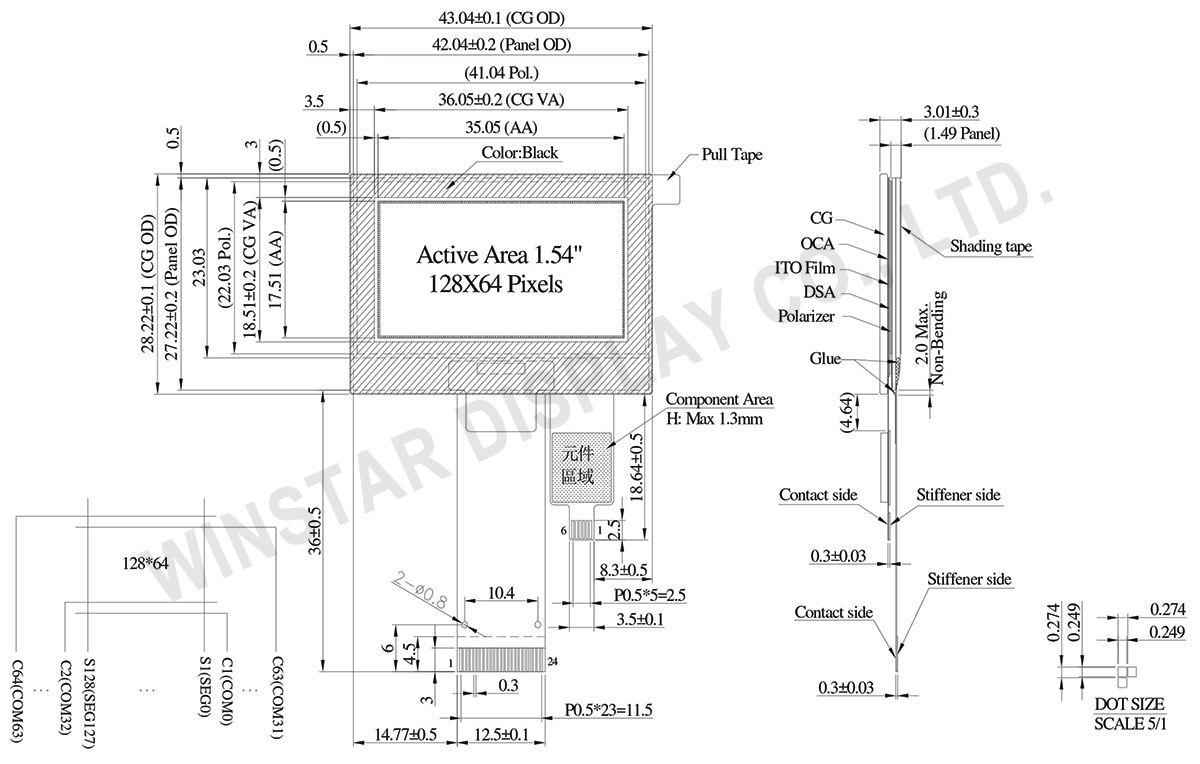
| 模組尺寸 | 43.04 × 28.22 × 3.01 | mm |
| 有效區域 | 35.05 × 17.51 | mm |
| 像素大小 | 0.249 × 0.249 | mm |
| 像素間距 | 0.274 × 0.274 | mm |
| 顯示模式 | 被動矩陣 | |
| 顯示顏色 | 單色 | |
| 驅動方式 | 1/64 Duty | |
| IC | SSD1309 | |
| 介面 | 6800,8080,4線SPI,I2C | |
| 尺寸 | 1.54 吋 | |
| CTP IC | FT6336U | |
| 支援手指數 | 1 | |
| CTP 介面 | I2C | |
| 表面 | 亮面 | |
| 參數 | 符號 | 最小值 | 最大值 | 單位 |
|---|---|---|---|---|
| 邏輯電源電壓 | VDD | -0.3 | 4 | V |
| 顯示電源電壓 | VCC | 0 | 17 | V |
| 工作溫度 | TOP | -10 | +60 | °C |
| 儲存溫度 | TSTG | -20 | +70 | °C |
| 參數 | 符號 | 最小值 | 最大值 | 單位 |
|---|---|---|---|---|
| 供電電壓 | VDD | 0 | 3.6 | V |
| 項目 | 符號 | 條件 | 最小值 | 典型值 | 最大值 | 單位 |
|---|---|---|---|---|---|---|
| 邏輯電源電壓 | VDD | - | 2.8 | 3.0 | 3.3 | V |
| 顯示電源電壓 | VCC | - | 7.0 | 12.5 | 13.0 | V |
| 輸入高準位 | VIH | - | 0.8×VDD | - | - | V |
| 輸入低準位 | VIL | - | - | - | 0.2×VDD | V |
| 輸出高準位 | VOH | - | 0.9×VDD | - | - | V |
| 輸出低準位 | VOL | - | - | - | 0.1×VDD | V |
| 50%顯示畫面耗電流 | VCC =12.5V | - | 15 | 30 | mA | |
| 項目 | 符號 | 條件 | 最小值 | 典型值 | 最大值 | 單位 |
|---|---|---|---|---|---|---|
| 電源電壓 | VDD | - | 2.8 | 3.0 | 3.3 | V |
| 輸入高準位 | VIH | - | 0.7×VDD | - | VDD | V |
| 輸入低準位 | VIL | - | -0.3 | - | 0.3×VDD | V |
| 輸出高準位 | VOH | - | 0.7×VDD | - | - | V |
| 輸出低準位 | VOL | - | - | - | 0.3×VDD | V |
| 產品圖 | 型號 | OLED IC | OLED 介面 | TP IC | TP 介面 | TP 支援手指數 | TP 貼合方式 |
|---|---|---|---|---|---|---|---|
 |
WEO012864AWPP3A00000 | SSD1309 | 6800,8080,4-wire SPI,I2C | FT6336U | I2C | 1 | OCA Optical-Bonding 光學貼合 |
 |
WEO012864AWPP3D00001 | SSD1309 | 6800,8080,4-wire SPI,I2C | FT6336U | I2C | 1 | Air-Bonding 口字貼合 |
| No. | 符號 | 功能說明 | |||||||||||||||
|---|---|---|---|---|---|---|---|---|---|---|---|---|---|---|---|---|---|
| 1 | NC(GND) | No connection | |||||||||||||||
| 2 | VLSS | This is an analog ground pin | |||||||||||||||
| 3 | VSS | Ground. | |||||||||||||||
| 4 | NC | No connection | |||||||||||||||
| 5 | VDD | Power supply pin for core logic operation | |||||||||||||||
| 6 | BS1 | MCU bus interface selection pins. Select appropriate logic setting as described in the following table. BS2 and BS1 are pin select
(1) 0 is connected to VSS (2) 1 is connected to VDD |
|||||||||||||||
| 7 | BS2 | ||||||||||||||||
| 8 | CS# | This pin is the chip select input connecting to the MCU. The chip is enabled for MCU communication only when CS# is pulled LOW (active LOW). |
|||||||||||||||
| 9 | RES# | This pin is reset signal input. When the pin is pulled LOW, initialization of the chip is executed. Keep this pin pull HIGH during normal operation. |
|||||||||||||||
| 10 | D/C# | This pin is Data/Command control pin connecting to the MCU. When the pin is pulled HIGH, the data at D[7:0] will be interpreted as data. When the pin is pulled LOW, the data at D[7:0] will be transferred to a command register. In I2C mode, this pin acts as SA0 for slave address selection. |
|||||||||||||||
| 11 | R/W# | This pin is read / write control input pin connecting to the MCU interface. When 6800 interface mode is selected, this pin will be used as Read/Write (R/W#) selection input. Read mode will be carried out when this pin is pulled HIGH and write mode when LOW. When 8080 interface mode is selected, this pin will be the Write (WR#) input. Data write operation is initiated when this pin is pulled LOW and the chip is selected. When serial or I2C interface is selected, this pin must be connected to VSS. |
|||||||||||||||
| 12 | E/RD# | This pin is MCU interface input. When 6800 interface mode is selected, this pin will be used as the Enable (E) signal. Read/write operation is initiated when this pin is pulled HIGH and the chip is selected. When 8080 interface mode is selected, this pin receives the Read (RD#) signal. Read operation is initiated when this pin is pulled LOW and the chip is selected. When serial or I2C interface is selected, this pin must be connected to VSS. |
|||||||||||||||
| 13-20 | D0~D7 | These pins are bi-directional data bus connecting to the MCU data bus. Unused pins are recommended to tie LOW. When serial interface mode is selected, D0 will be the serial clock input: SCLK; D1 will be the serial data input: SDIN and D2 should be kept NC. When I2C mode is selected, D2, D1 should be tied together and serve as SDAout, SDAin in application and D0 is the serial clock input, SCL. |
|||||||||||||||
| 21 | IREF | This pin is the segment output current reference pin. IREF is supplied externally. |
|||||||||||||||
| 22 | VCOMH | COM signal deselected voltage level. A capacitor should be connected between this pin and VSS. |
|||||||||||||||
| 23 | VCC | Power supply for panel driving voltage. This is also the most positive power voltage supply pin. | |||||||||||||||
| 24 | NC(GND) | No connection |
| 1 | GND | Ground. |
| 2 | VDD | Power Supply Voltage of CTP |
| 3 | RST | External Reset, Low is active |
| 4 | INT | External interrupt to the host |
| 5 | SCL | I2C clock input |
| 6 | SDA | I2C data input and output |

通過點擊「允許所有 Cookie」,代表您同意在您的設備上存儲 Cookie 以增強網站瀏覽體驗、分析網站使用情況並協助我們的行銷和網站效能優化工作。您可以在我們的隱私權政策中找到有關於此的更多資訊。