


我們重視您的隱私
通過點擊「允許所有 Cookie」,代表您同意在您的設備上存儲 Cookie 以增強網站瀏覽體驗、分析網站使用情況並協助我們的行銷和網站效能優化工作。您可以在我們的隱私權政策中找到有關於此的更多資訊。


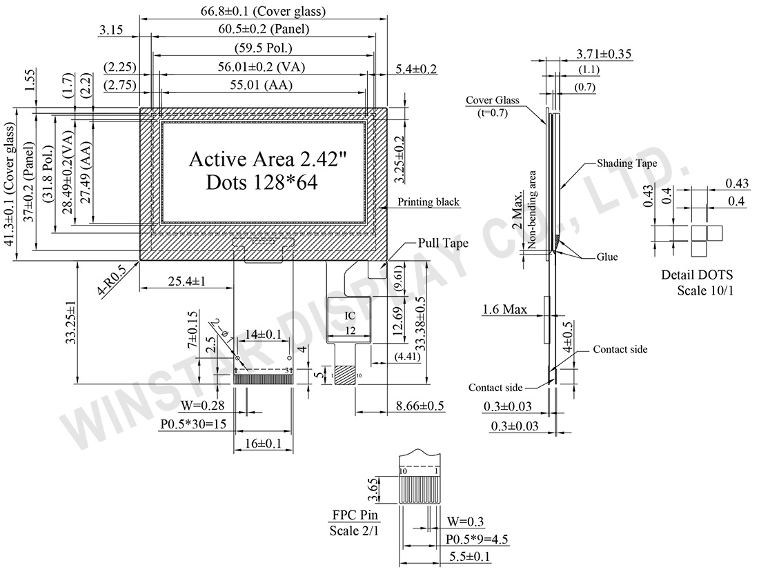
WEO012864G是最多工控產品應用所採用的COG OLED顯示器模組,尺寸2.42吋。我們推出此款帶電容式觸控面板(CTP)型號供客戶選用,面板解析度128x64點,內建SSD1309 IC,支援 6800/8080 8-bit 平行介面,I2C與4-線SPI介面,3V電壓驅動,1/64 duty。WEO012864G電容式觸控面板內建GT911 IC,支援I2C介面,單點觸控。此OLED模組具有10,000:1的高對比度,影像顯示更清晰。
此款含電容觸控面板模組是COG結構OLED,非常適用於智慧家電、智能檢測、能源系統、量測儀器、POS系統、智能醫療設備等產品。模組工作溫度是-20℃至 70℃,儲存溫度-30℃至 80℃。
| 項目 | 規格 | 單位 |
|---|---|---|
| 點陣(解析度) | 128 x 64 | Dot |
| 模組尺寸 | 66.8 × 41.3 × 3.71 | mm |
| 有效區域 | 55.01 × 27.49 | mm |
| 點大小 | 0.40 × 0.40 | mm |
| 點間距 | 0.43 × 0.43 | mm |
| 顯示模式 | 被動矩陣 | |
| 發光顏色 | 單色 | |
| 介面 | 8Bits 68xx 80xx / 4線 SPI / I2C | |
| 驅動方式 | 1/64 Duty | |
| OLED IC | SSD1309 | |
| 尺寸 | 2.42 吋 | |
| CTP IC | GT911 | |
| 支援手指數 | 1 | |
| CTP介面 | I2C | |
| 表面 | 亮面 | |
| 參數 | 符號 | 最小值 | 最大值 | 單位 |
|---|---|---|---|---|
| 邏輯電源電壓 | VDD | -0.3 | 4 | V |
| 顯示電源電壓 | VCC | 0 | 15 | V |
| 工作溫度 | TOP | -20 | +70 | °C |
| 儲存溫度 | TSTG | -30 | +80 | °C |
| 參數 | 符號 | 最小值 | 最大值 | 單位 |
|---|---|---|---|---|
| 電源電壓 | VDD | 2.66 | 3.47 | V |
| 項目 | 符號 | 條件 | 最小值 | 典型值 | 最大值 | 單位 |
|---|---|---|---|---|---|---|
| 邏輯電源電壓 | VDD | - | 2.8 | 3.0 | 3.3 | V |
| 顯示電源電壓 | VCC | - | 12.5 | 13.0 | 13.5 | V |
| 輸入高準位 | VIH | - | 0.8×VDD | - | - | V |
| 輸入低準位 | VIL | - | - | - | 0.2×VDD | V |
| 輸出高準位 | VOH | - | 0.9×VDD | - | - | V |
| 輸出低準位 | VOL | - | - | - | 0.1×VDD | V |
| 50%顯示畫面耗電流 | VCC =13.0V | - | 25 | 36 | mA | |
| 項目 | 符號 | 最小值 | 典型值 | 最大值 | 單位 |
|---|---|---|---|---|---|
| 電源電壓 | VDD | 2.8 | 3.0 | 3.3 | V |
| 輸入高電壓 | VIH | 0.75xVDD | VDD+0.3 | V | |
| 輸入低電壓 | VIL | -0.3 | - | 0.25xVDD | V |
| 輸出高電壓 | VOH | 0.85xVDD | - | - | V |
| 輸出低電壓 | VOL | - | - | 0.15xVDD | V |
| No. | 符號 | 說明 | |||||||||||||||
|---|---|---|---|---|---|---|---|---|---|---|---|---|---|---|---|---|---|
| 1 | NC(GND) | No connection | |||||||||||||||
| 2 | VSS | Ground. | |||||||||||||||
| 3-10 | NC | No connection | |||||||||||||||
| 11 | VDD | Power supply pin for core logic operation | |||||||||||||||
| 12 | BS1 | MCU bus interface selection pins. Select appropriate logic setting as described in the following table. BS2, BS1 and BS0 are pin select
(1) 0 is connected to VSS (2) 1 is connected to VDD |
|||||||||||||||
| 13 | BS2 | ||||||||||||||||
| 14 | NC | No connection | |||||||||||||||
| 15 | CS# | This pin is the chip select input connecting to the MCU. The chip is enabled for MCU communication only when CS# is pulled LOW (active LOW). |
|||||||||||||||
| 16 | RES# | This pin is reset signal input. When the pin is pulled LOW, initialization of the chip is executed. Keep this pin pull HIGH during normal operation. |
|||||||||||||||
| 17 | D/C# | This pin is Data/Command control pin connecting to the MCU. When the pin is pulled HIGH, the data at D[7:0] will be interpreted as data. When the pin is pulled LOW, the data at D[7:0] will be transferred to a command register. In I2C mode, this pin acts as SA0 for slave address selection. |
|||||||||||||||
| 18 | R/W# | This pin is read / write control input pin connecting to the MCU interface. When 6800 interface mode is selected, this pin will be used as Read/Write (R/W#) selection input. Read mode will be carried out when this pin is pulled HIGH and write mode when LOW. When 8080 interface mode is selected, this pin will be the Write (WR#) input. Data write operation is initiated when this pin is pulled LOW and the chip is selected. When serial or I2C interface is selected, this pin must be connected to VSS. |
|||||||||||||||
| 19 | E/RD# | This pin is MCU interface input. When 6800 interface mode is selected, this pin will be used as the Enable (E) signal. Read/write operation is initiated when this pin is pulled HIGH and the chip is selected. When 8080 interface mode is selected, this pin receives the Read (RD#) signal. Read operation is initiated when this pin is pulled LOW and the chip is selected. When serial or I2C interface is selected, this pin must be connected to VSS. |
|||||||||||||||
| 20~27 | D0~D7 | These pins are bi-directional data bus connecting to the MCU data bus. Unused pins are recommended to tie LOW. When serial interface mode is selected, D0 will be the serial clock input: SCLK; D1 will be the serial data input: SDIN and D2 should be kept NC. When I2C mode is selected, D2, D1 should be tied together and serve as SDAout, SDAin in application and D0 is the serial clock input, SCL. |
|||||||||||||||
| 28 | IREF | This pin is the segment output current reference pin. IREF is supplied externally. |
|||||||||||||||
| 29 | VCOMH | COM signal deselected voltage level. A capacitor should be connected between this pin and VSS. |
|||||||||||||||
| 30 | VCC | Power supply for panel driving voltage. This is also the most positive power voltage supply pin. | |||||||||||||||
| 31 | NC(GND) | No connection |
| No. | 符號 | 說明 |
|---|---|---|
| 1 | GND | Power ground |
| 2 | VDD | Power supply |
| 3 | INT | Interrupt signal, active low, asserted to request Host start a new transaction |
| 4 | SDA | I2C data signal |
| 5 | SCL | I2C clock signal |
| 6 | RST | External reset signal, active low |
| 7 | GND | Power ground |
| 8 | GND | Power ground |
| 9 | GND | Power ground |
| 10 | GND | Power ground |

通過點擊「允許所有 Cookie」,代表您同意在您的設備上存儲 Cookie 以增強網站瀏覽體驗、分析網站使用情況並協助我們的行銷和網站效能優化工作。您可以在我們的隱私權政策中找到有關於此的更多資訊。