
- WEA012864A")
我们重视您的隐私
通过点击「允许所有 Cookie」,代表您同意在您的设备上存储 Cookie 以增强网站浏览体验、分析网站使用情况并协助我们的营销和网站效能优化工作。您可以在我们的隐私权政策中找到有关于此的更多信息。


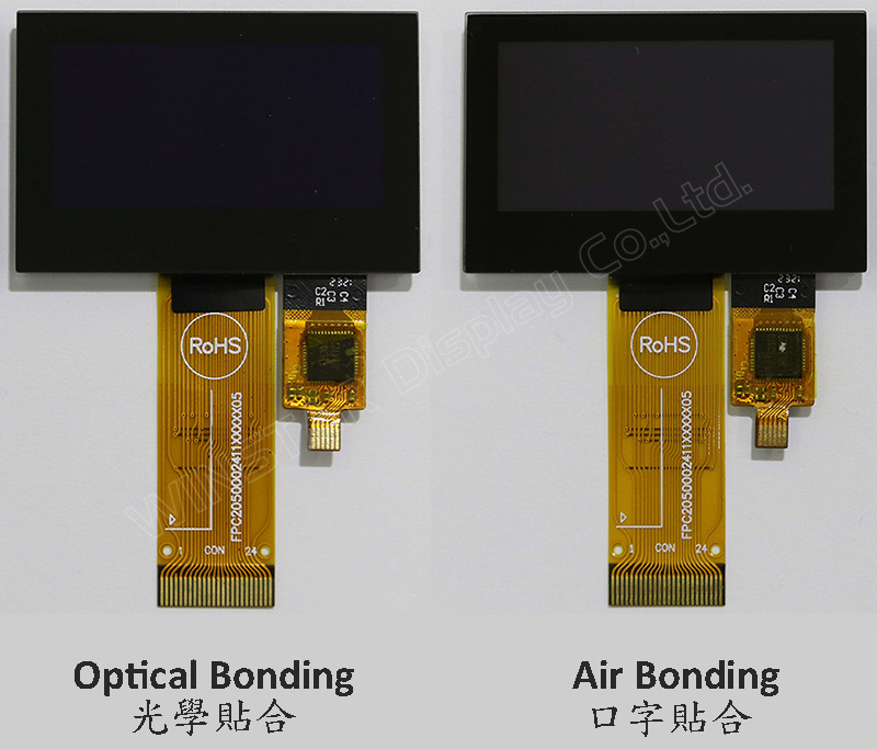
WEO012864A-CTP是一款1.54吋COG结构绘图型OLED显示器模块搭载CTP电容式触控面板,分辨率为128x64像素,内建SSD1309 IC,支持6800/8080 8-bit并列传输接口、4线SPI及I2C接口;逻辑电源电压为 2.8V ~ 3.3V,Typical 值为3.0V,显示器电源电压 12.5V,驱动方式1/64。此型号提供两种 CTP 结构选项;一种为采用口字贴合 (Air Bonding) 技术的CTP触控面板,另一选项为采用光学贴合 (Optical Bonding) 技术的CTP触控面板,此两种CTP触控面板触控IC皆使用FT6336U,均支持I2C接口和单点触控。
WEO012864A型号搭载CTP触控面板非常适用于智能家居应用、智能技术设备、仪表装置、工业控制系统、医疗仪器…等。此模块工作温度范围为-10℃~+60℃;储存温度范围为-20℃~+70℃。
WEO012864A-CTP 型号 OLED 模块具有 10,000:1 的高对比度度,可呈现更鲜艳、更深的黑色以及更明亮的白色。 这样可以提高影像质量、更清晰的细节并提高可读性。
| 项目 | 规格说明 | 单位 |
|---|---|---|
| 点阵(分辨率) | 128 x 64 | - |
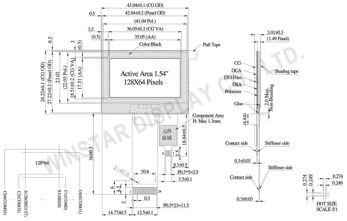
| 模块尺寸 | 43.04 × 28.22 × 3.01 | mm |
| 有效区域 | 35.05 × 17.51 | mm |
| 像素大小 | 0.249 × 0.249 | mm |
| 像素间距 | 0.274 × 0.274 | mm |
| 显示模式 | 被动矩阵 | |
| 显示颜色 | 单色 | |
| 驱动方式 | 1/64 Duty | |
| IC | SSD1309 | |
| 接口 | 6800,8080,4线SPI,I2C | |
| 尺寸 | 1.54 寸 | |
| CTP IC | FT6336U | |
| 支援手指数 | 1 | |
| CTP 接口 | I2C | |
| 表面 | 亮面 | |
| 参数 | 符号 | 最小值 | 最大值 | 单位 |
|---|---|---|---|---|
| 逻辑电源电压 | VDD | -0.3 | 4 | V |
| 显示电源电压 | VCC | 0 | 17 | V |
| 工作温度 | TOP | -10 | +60 | °C |
| 储存温度 | TSTG | -20 | +70 | °C |
| 参数 | 符号 | 最小值 | 最大值 | 单位 |
|---|---|---|---|---|
| 供电电压 | VDD | 0 | 3.6 | V |
| 项目 | 符号 | 条件 | 最小值 | 典型值 | 最大值 | 单位 |
|---|---|---|---|---|---|---|
| 逻辑电源电压 | VDD | - | 2.8 | 3.0 | 3.3 | V |
| 显示电源电压 | VCC | - | 7.0 | 12.5 | 13.0 | V |
| 输入高准位 | VIH | - | 0.8×VDD | - | - | V |
| 输入低准位 | VIL | - | - | - | 0.2×VDD | V |
| 输出高准位 | VOH | - | 0.9×VDD | - | - | V |
| 输出低准位 | VOL | - | - | - | 0.1×VDD | V |
| 50%显示画面耗电流 | VCC =12.5V | - | 15 | 30 | mA | |
| 项目 | 符号 | 条件 | 最小值 | 典型值 | 最大值 | 单位 |
|---|---|---|---|---|---|---|
| 电源电压 | VDD | - | 2.8 | 3.0 | 3.3 | V |
| 输入高准位 | VIH | - | 0.7×VDD | - | VDD | V |
| 输入低准位 | VIL | - | -0.3 | - | 0.3×VDD | V |
| 输出高准位 | VOH | - | 0.7×VDD | - | - | V |
| 输出低准位 | VOL | - | - | - | 0.3×VDD | V |
| 产品图 | 型号 | OLED IC | OLED 接口 | TP IC | TP 接口 | TP 支援手指数 | TP 贴合方式 |
|---|---|---|---|---|---|---|---|
 |
WEO012864AWPP3A00000 | SSD1309 | 6800,8080,4-wire SPI,I2C | FT6336U | I2C | 1 | OCA Optical-Bonding 光学贴合 |
 |
WEO012864AWPP3D00001 | SSD1309 | 6800,8080,4-wire SPI,I2C | FT6336U | I2C | 1 | Air-Bonding 口字贴合 |
| No. | 符号 | 功能说明 | |||||||||||||||
|---|---|---|---|---|---|---|---|---|---|---|---|---|---|---|---|---|---|
| 1 | NC(GND) | No connection | |||||||||||||||
| 2 | VLSS | This is an analog ground pin | |||||||||||||||
| 3 | VSS | Ground. | |||||||||||||||
| 4 | NC | No connection | |||||||||||||||
| 5 | VDD | Power supply pin for core logic operation | |||||||||||||||
| 6 | BS1 | MCU bus interface selection pins. Select appropriate logic setting as described in the following table. BS2 and BS1 are pin select
(1) 0 is connected to VSS (2) 1 is connected to VDD |
|||||||||||||||
| 7 | BS2 | ||||||||||||||||
| 8 | CS# | This pin is the chip select input connecting to the MCU. The chip is enabled for MCU communication only when CS# is pulled LOW (active LOW). |
|||||||||||||||
| 9 | RES# | This pin is reset signal input. When the pin is pulled LOW, initialization of the chip is executed. Keep this pin pull HIGH during normal operation. |
|||||||||||||||
| 10 | D/C# | This pin is Data/Command control pin connecting to the MCU. When the pin is pulled HIGH, the data at D[7:0] will be interpreted as data. When the pin is pulled LOW, the data at D[7:0] will be transferred to a command register. In I2C mode, this pin acts as SA0 for slave address selection. |
|||||||||||||||
| 11 | R/W# | This pin is read / write control input pin connecting to the MCU interface. When 6800 interface mode is selected, this pin will be used as Read/Write (R/W#) selection input. Read mode will be carried out when this pin is pulled HIGH and write mode when LOW. When 8080 interface mode is selected, this pin will be the Write (WR#) input. Data write operation is initiated when this pin is pulled LOW and the chip is selected. When serial or I2C interface is selected, this pin must be connected to VSS. |
|||||||||||||||
| 12 | E/RD# | This pin is MCU interface input. When 6800 interface mode is selected, this pin will be used as the Enable (E) signal. Read/write operation is initiated when this pin is pulled HIGH and the chip is selected. When 8080 interface mode is selected, this pin receives the Read (RD#) signal. Read operation is initiated when this pin is pulled LOW and the chip is selected. When serial or I2C interface is selected, this pin must be connected to VSS. |
|||||||||||||||
| 13-20 | D0~D7 | These pins are bi-directional data bus connecting to the MCU data bus. Unused pins are recommended to tie LOW. When serial interface mode is selected, D0 will be the serial clock input: SCLK; D1 will be the serial data input: SDIN and D2 should be kept NC. When I2C mode is selected, D2, D1 should be tied together and serve as SDAout, SDAin in application and D0 is the serial clock input, SCL. |
|||||||||||||||
| 21 | IREF | This pin is the segment output current reference pin. IREF is supplied externally. |
|||||||||||||||
| 22 | VCOMH | COM signal deselected voltage level. A capacitor should be connected between this pin and VSS. |
|||||||||||||||
| 23 | VCC | Power supply for panel driving voltage. This is also the most positive power voltage supply pin. | |||||||||||||||
| 24 | NC(GND) | No connection |
| 1 | GND | Ground. |
| 2 | VDD | Power Supply Voltage of CTP |
| 3 | RST | External Reset, Low is active |
| 4 | INT | External interrupt to the host |
| 5 | SCL | I2C clock input |
| 6 | SDA | I2C data input and output |

通过点击「允许所有 Cookie」,代表您同意在您的设备上存储 Cookie 以增强网站浏览体验、分析网站使用情况并协助我们的营销和网站效能优化工作。您可以在我们的隐私权政策中找到有关于此的更多信息。