 - WEN025664A")
我们重视您的隐私
通过点击「允许所有 Cookie」,代表您同意在您的设备上存储 Cookie 以增强网站浏览体验、分析网站使用情况并协助我们的营销和网站效能优化工作。您可以在我们的隐私权政策中找到有关于此的更多信息。
 - WEN025664A-CTP")
 - WEN025664A-CTP")
 - WEN025664A-CTP")
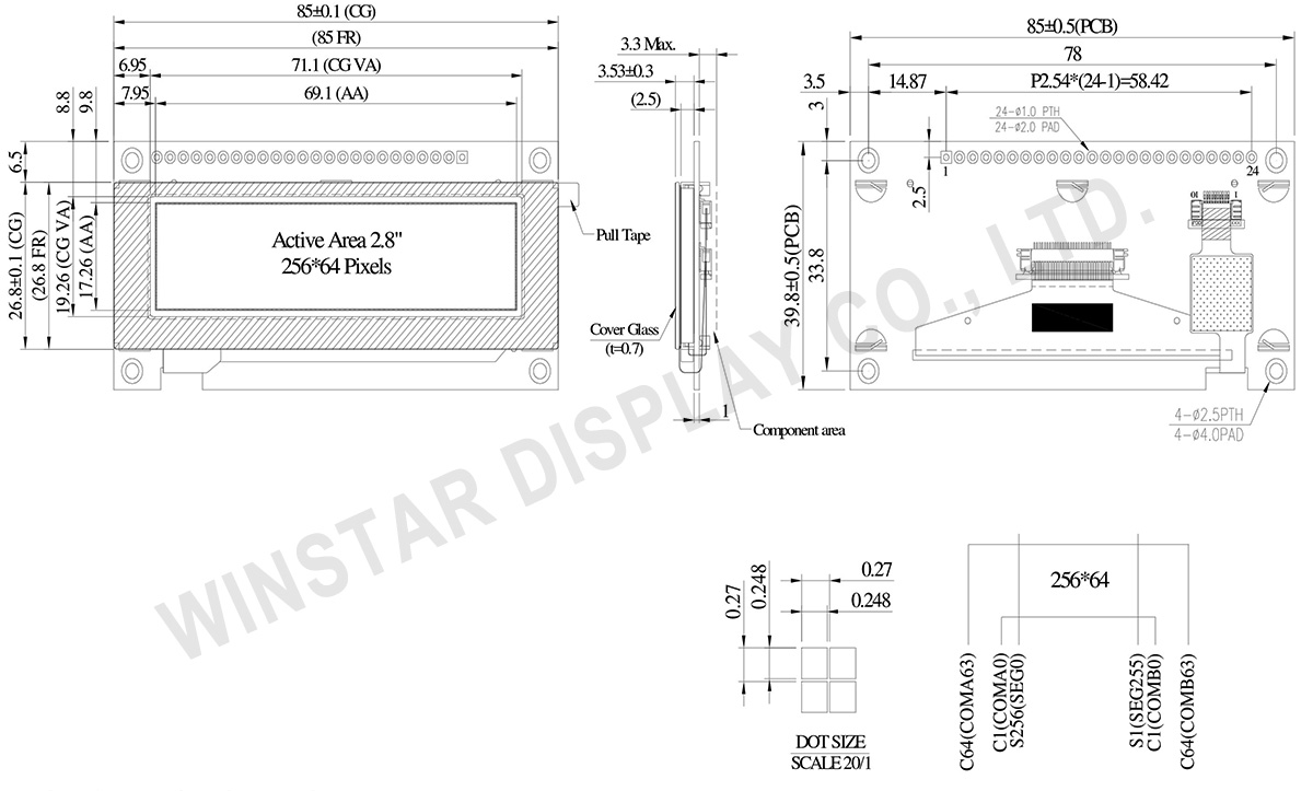
WEN025664A-CTP是一款2.8英寸单色图形COF OLED显示模块,集成投射式电容触控面板(PCAP),分辨率为256×64 dots。该模块采用SSD1322驱动IC,支持6800/8080 8-bit并行接口以及3/4线SPI接口。模块外形尺寸为85.0 × 39.8 mm,显示区域为69.1 × 17.26 mm。触控面板采用FT6336U控制器,支持I²C接口及单点触控。
该OLED显示模块工作电压为3V,采用1/64 duty驱动方式,支持灰度显示,对比度可达10,000:1。工作温度范围为-20°C至+70°C,存储温度范围为-30°C至+80°C。
WEN025664A-CTP采用金属框架与PCB一体化设计,并提供4个安装孔,便于进行机械结构整合。由于接口配置及VDD电源电路已集成于PCB上,模块可通过线材直接连接至系统,有助于简化系统设计并减少额外转接板的使用。
WEN025664A-CTP系列同时提供无触控版本。如需无触控面板方案,请参考WEN025664A系列。
| 项目 | 尺寸 | 单位 |
|---|---|---|
| 点阵 | 256 × 64 Dots | - |
| 模块尺寸 | 85.0 × 39.8 ×7.83 | mm |
| 有效区域 | 69.1 × 17.26 | mm |
| 点大小 | 0.248×0.248 | mm |
| 点间距 | 0.27×0.27 | mm |
| 显示模式 | 被动矩阵 | |
| 发光颜色 | 单色 | |
| 驱动方式 | 1/64 Duty | |
| OLED IC | SSD1322 (COF) | |
| OLED 接口 | 6800, 8080, SPI | |
| 尺寸(对角线) | 2.8 寸 | |
| CTP IC | FT6336U | |
| 支援手指数 | 1 | |
| CTP 接口 | I2C | |
| 表面 | 亮面 | |
| 参数 | 符号 | 最小值 | 最大值 | 单位 |
|---|---|---|---|---|
| 显示电源电压 | VDD | -0.3 | 4 | V |
| 工作温度 | TOP | -20 | +70 | °C |
| 储存温度 | TSTG | -30 | +80 | °C |
| 项目 | 符号 | 条件 | 最小值 | 典型值 | 最大值 | 单位 |
|---|---|---|---|---|---|---|
| 逻辑电源电压 | VDD | - | 2.8 | 3.0 | 3.3 | V |
| 输入高准位 | VIH | - | 0.8×VDD | - | VDD | V |
| 输入低准位 | VIL | - | 0 | - | 0.2×VDD | V |
| 输出高准位 | VOH | - | 0.9×VDD | - | VDD | V |
| 输出低准位 | VOL | - | 0 | - | 0.1×VDD | V |
| 50%显示画面耗电流 | IDD | VDD =3V | - | 125 | 250 | mA |
| Pin Number | 符号 | I/O | 功能说明 | ||||||||||
|---|---|---|---|---|---|---|---|---|---|---|---|---|---|
| 1 | VSS | P | Ground. | ||||||||||
| 2 | VDD | P | Power Supply for Core Logic Circuit Power supply pin for core logic operation. A capacitor is required to connect between this pin and VSS |
||||||||||
| 3 | N.C. | P | Reserved Pin The N.C. pin between function pins are reserved for compatible and flexible design. |
||||||||||
| 4 | D/C# | I | Data/Command Control This pin is Data/Command control pin connecting to the MCU. When the pin is pulled HIGH, the content at D[7:0] will be interpreted as data. When the pin is pulled LOW, the content at D[7:0] will be interpreted as command. |
||||||||||
| 5 | R/W# (WR#) |
I | Read/Write Select or Write This pin is MCU interface input. When interfacing to a 68XX-series microprocessor, this pin will be used as Read/Write (R/W#) selection input. Pull this pin to “High” for read mode and pull it to “Low” for write mode. When 80XX interface mode is selected, this pin will be the Write (WR#) input. Data write operation is initiated when this pin is pulled low and the CS# is pulled low. When serial mode is selected, this pin must be connected to VSS. |
||||||||||
| 6 | E/RD# | I | Read/Write Enable or Read This pin is MCU interface input. When interfacing to a 68XX-series microprocessor, this pin will be used as the Enable (E) signal. Read/write operation is initiated when this pin is pulled high and the CS# is pulled low. When connecting to an 80XX-microprocessor, this pin receives the Read (RD#) signal. Data read operation is initiated when this pin is pulled low and CS# is pulled low. When serial mode is selected, this pin must be connected to VSS. |
||||||||||
| 7~14 | DB0 | I/O | Host Data Input/Output Bus These pins are 8-bit bi-directional data bus to be connected to the microprocessor’s data bus. When serial mode is selected, D1 will be the serial data input SDIN and D0 will be the serial clock input SCLK. |
||||||||||
| DB1 | |||||||||||||
| DB2 | |||||||||||||
| DB3 | |||||||||||||
| DB4 | |||||||||||||
| DB5 | |||||||||||||
| DB6 | |||||||||||||
| DB7 | |||||||||||||
| 15 | NC | P | Reserved Pin The N.C. pin between function pins are reserved for compatible and flexible design. |
||||||||||
| 16 | RES# | I | This pin is reset signal input. When the pin is pulled LOW, initialization of the chip is executed. Keep this pin pull HIGH during normal operation. |
||||||||||
| 17 | CS# | I | Data/Command Control This pin is the chip select input connecting to the MCU. The chip is enabled for MCU communication only when CS# is pulled LOW. |
||||||||||
| 18 | NC | P | Reserved Pin The N.C. pin between function pins are reserved for compatible and flexible design. |
||||||||||
| 19 | BS1 | I | Communicating Protocol Select These pins are MCU interface selection input. See the following table:
Note (1) 0 is connected to VSS (2) 1 is connected to VDD |
||||||||||
| 20 | BS0 | ||||||||||||
| 21 | TP_SCK | I | I2C clock input | ||||||||||
| 22 | TP_SDA | I | I2C data input and output | ||||||||||
| 23 | TP_INT | I | External interrupt to the host | ||||||||||
| 24 | TP_RST | I | External Reset, Low is active |

通过点击「允许所有 Cookie」,代表您同意在您的设备上存储 Cookie 以增强网站浏览体验、分析网站使用情况并协助我们的营销和网站效能优化工作。您可以在我们的隐私权政策中找到有关于此的更多信息。