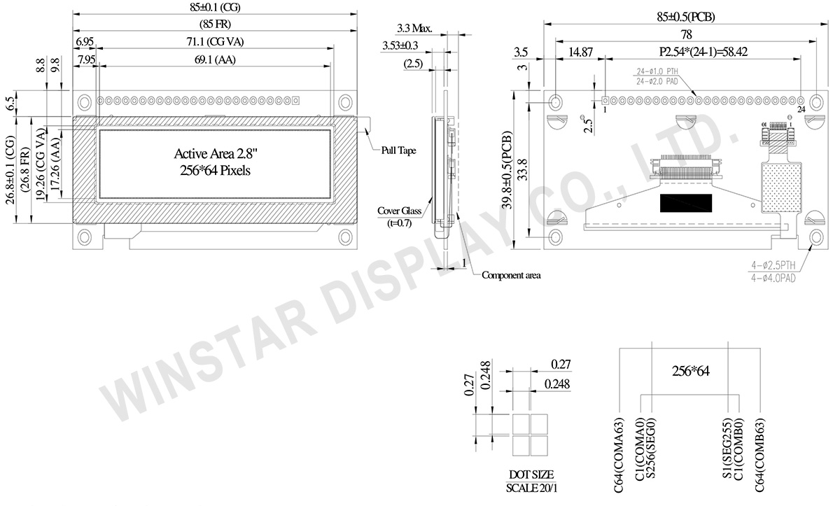
Ecrã OLED COF em tons de cinza de 2,8 polegadas com resolução de 256x64, painel tátil, PCB e suporte de moldura
Model No. WEN025664A-CTP
►Tipo: Gráfico
►Estrutura: COF + Frame + PCB
►Tamanho: 2,8 polegadas
►Matriz de pontos 256×64
►IC:SSD1322
►Alimentação +3V
►1/64 duty cycle
►Interface: 6800, 8080, SPI
►Tela de Toque: Com painel de toque capacitivo (CTP)
►Detect Point : 1 Finger
►Display Color: Branco / Amarelo
►Support Grayscale
Descrição
A série WEN025664A-CTP é um display COF OLED gráfico monocromático de 2,8 polegadas, com um painel capacitivo sensível ao toque e uma resolução de 256x64 pontos. Equipado com o IC SSD1322, suporta várias interfaces, incluindo 6800/8080 de 8 bits e interfaces SPI de 3/4 fios. As dimensões do módulo do WEN025664A-CTP são 85,0 × 39,8 mm, e a área ativa é 69,1 × 17,26 mm. O modelo incorpora um painel capacitivo sensível ao toque projetado (PCAP) com o IC FT6336U, suportando interfaces I2C e toque de 1 ponto.
A série OLED WEN025664A-CTP opera com uma alimentação de 3V e um método de acionamento de 1/64. Suporta tons de cinza e possui uma alta taxa de contraste de 10.000:1. O módulo é capaz de funcionar em temperaturas que variam de -20°C a +70°C, com uma faixa de temperatura de armazenamento de -30°C a +80°C.
Com uma estrutura metálica, uma placa de circuito (PCB) e quatro furos para parafusos, o WEN025664A-CTP facilita a instalação para os clientes. A série OLED, equipada com uma placa de circuito, pode se conectar facilmente a aplicações usando fios, eliminando a necessidade de os clientes desenvolverem placas de circuito adicionais. A integração de configurações de interface e circuitos VDD aprimora a facilidade de uso. Além disso, os quatro furos para parafusos na PCB simplificam o processo de instalação no produto aplicativo.
O WEN025664A-CTP também oferece uma opção com o mesmo painel OLED, mas sem um painel sensível ao toque. Por favor, escolha o Modelo WEN025664A para a opção sem painel sensível ao toque.
DRAWING
Data source ref: WEN025664AWPP3D00000
SPECIFICATIONS
Função do pino de interface
Pin Number | Símbolo | I/O | Função | ||||||||||
---|---|---|---|---|---|---|---|---|---|---|---|---|---|
1 | VSS | P | Ground. | ||||||||||
2 | VDD | P | Power Supply for Core Logic Circuit Power supply pin for core logic operation. A capacitor is required to connect between this pin and VSS |
||||||||||
3 | N.C. | P | Reserved Pin The N.C. pin between function pins are reserved for compatible and flexible design. |
||||||||||
4 | D/C# | I | Data/Command Control This pin is Data/Command control pin connecting to the MCU. When the pin is pulled HIGH, the content at D[7:0] will be interpreted as data. When the pin is pulled LOW, the content at D[7:0] will be interpreted as command. |
||||||||||
5 | R/W# (WR#) |
I | Read/Write Select or Write This pin is MCU interface input. When interfacing to a 68XX-series microprocessor, this pin will be used as Read/Write (R/W#) selection input. Pull this pin to “High” for read mode and pull it to “Low” for write mode. When 80XX interface mode is selected, this pin will be the Write (WR#) input. Data write operation is initiated when this pin is pulled low and the CS# is pulled low. When serial mode is selected, this pin must be connected to VSS. |
||||||||||
6 | E/RD# | I | Read/Write Enable or Read This pin is MCU interface input. When interfacing to a 68XX-series microprocessor, this pin will be used as the Enable (E) signal. Read/write operation is initiated when this pin is pulled high and the CS# is pulled low. When connecting to an 80XX-microprocessor, this pin receives the Read (RD#) signal. Data read operation is initiated when this pin is pulled low and CS# is pulled low. When serial mode is selected, this pin must be connected to VSS. |
||||||||||
7~14 | DB0 | I/O | Host Data Input/Output Bus These pins are 8-bit bi-directional data bus to be connected to the microprocessor’s data bus. When serial mode is selected, D1 will be the serial data input SDIN and D0 will be the serial clock input SCLK. |
||||||||||
DB1 | |||||||||||||
DB2 | |||||||||||||
DB3 | |||||||||||||
DB4 | |||||||||||||
DB5 | |||||||||||||
DB6 | |||||||||||||
DB7 | |||||||||||||
15 | NC | P | Reserved Pin The N.C. pin between function pins are reserved for compatible and flexible design. |
||||||||||
16 | RES# | I | This pin is reset signal input. When the pin is pulled LOW, initialization of the chip is executed. Keep this pin pull HIGH during normal operation. |
||||||||||
17 | CS# | I | Data/Command Control This pin is the chip select input connecting to the MCU. The chip is enabled for MCU communication only when CS# is pulled LOW. |
||||||||||
18 | NC | P | Reserved Pin The N.C. pin between function pins are reserved for compatible and flexible design. |
||||||||||
19 | BS1 | I | Communicating Protocol Select These pins are MCU interface selection input. See the following table:
Note (1) 0 is connected to VSS (2) 1 is connected to VDD |
||||||||||
20 | BS0 | ||||||||||||
21 | TP_SCK | I | I2C clock input | ||||||||||
22 | TP_SDA | I | I2C data input and output | ||||||||||
23 | TP_INT | I | External interrupt to the host | ||||||||||
24 | TP_RST | I | External Reset, Low is active |
Especificações Gerais
Item | Dimensão | Unidade |
---|---|---|
Matriz de pontos | 256 x 64 pontos | - |
Dimensão do módulo | 85.0 × 39.8 ×7.83 | mm |
Área ativa | 69.1 × 17.26 | mm |
Tamanho do ponto | 0.248×0.248 | mm |
Distância entre pontos | 0.27×0.27 | mm |
Modo de exibição | Passive Matrix | |
Cor de exibição | Monochrome | |
Drive Duty | 1/64 Duty | |
OLED IC | SSD1322 (COF) | |
OLED Interface | 6800, 8080, SPI | |
Tamanho | 2,8 polegadas | |
CTP IC | FT6336U | |
Detect Point | 1 | |
CTP Interface | I2C | |
Superfície | Reflexo |
Classificações Máximas Absolutas
Parameter | Símbolo | Valor Min | Valor Máximo | Unidade |
---|---|---|---|---|
Supply Voltage for Display | VDD | -0.3 | 4 | V |
Temperatura de operação | TOP | -20 | +70 | °C |
Temperatura de armazenamento | TSTG | -30 | +80 | °C |
Características Eletrônicas
DC Características Eletrônicas
Item | Símbolo | Condição | Valor Min | Valor Típico | Valor Máximo | Unidade |
---|---|---|---|---|---|---|
Supply Voltage for Logic | VDD | - | 2.8 | 3.0 | 3.3 | V |
High Level Input | VIH | - | 0.8×VDD | - | VDD | V |
Low Level Input | VIL | - | 0 | - | 0.2×VDD | V |
High Level Output | VOH | - | 0.9×VDD | - | VDD | V |
Low Level Output | VOL | - | 0 | - | 0.1×VDD | V |
50% Check Board operating Current | IDD | VDD =3V | - | 125 | 250 | mA |