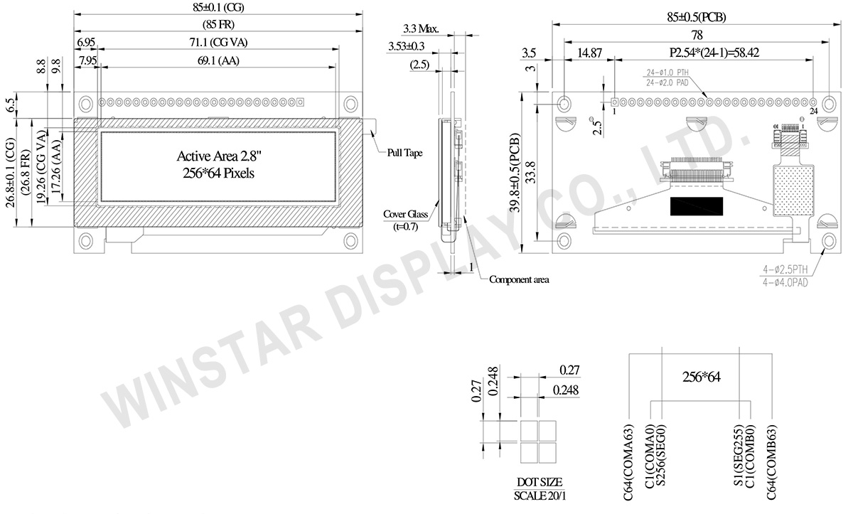
Home Prodotti Display OLED Display touch OLED WEN025664A-CTP

Display OLED COF in scala di grigi da 2,8 pollici con risoluzione 256x64, pannello touch, PCB e supporto cornice

Modello numero WEN025664A-CTP

►Tipo : grafico
►Struttura : COF + cornice + PCB
►Dimensione : 2.8 pollici
►256×64 a matrice di punti
►IC:SSD1322
►Alimentatore 3V
►1/64 duty cycle
►Interfaccia: 6800, 8080, SPI
►Touch Screen : con pannello touch capacitivo (CTP)
►Punti di tocco : 1 Dito
►Colore display: Bianco / Giallo
►Support Grayscale

Descrizione

La serie WEN025664A-CTP è un display OLED COF grafico monocromatico da 2,8 pollici con pannello capacitivo touch e risoluzione di 256x64 pixel. È dotato del chip SSD1322 e supporta diverse interfacce, tra cui 6800/8080 a 8 bit e interfacce SPI a 3/4 fili. Le dimensioni del modulo WEN025664A-CTP sono di 85,0 × 39,8 mm, e l'area attiva è di 69,1 × 17,26 mm. Il modello incorpora un pannello touch capacitivo proiettato (PCAP) con il chip FT6336U, che supporta interfacce I2C e il tocco a 1 punto.

La serie OLED WEN025664A-CTP opera con un'alimentazione a 3V e un metodo di guida di 1/64 di duty. Supporta le gradazioni di grigio e vanta un elevato rapporto di contrasto di 10.000:1. Il modulo è in grado di funzionare a temperature comprese tra -20°C e +70°C, con una temperatura di stoccaggio che varia da -30°C a +80°C.

Dotato di una cornice metallica con una scheda PCB e quattro fori per viti, il WEN025664A-CTP facilita l'installazione per i clienti. La serie OLED, dotata di una scheda PCB, può connettersi facilmente alle applicazioni tramite cavi, eliminando la necessità per i clienti di sviluppare ulteriori schede PCB. L'integrazione delle impostazioni dell'interfaccia e dei circuiti VDD migliora la facilità d'uso. Inoltre, i quattro fori per viti sulla PCB semplificano il processo di installazione sul prodotto applicativo.

Il WEN025664A-CTP offre anche un'opzione con lo stesso pannello OLED ma senza pannello touch. Si prega di scegliere il modello WEN025664A per l'opzione senza touch.

DISEGNO

2.8 inch 256x64 OLED Display with Touch Panel Support Grayscale - WEN025664A-CTP

Data source ref: WEN025664AWPP3D00000

SPECIFICHE TECNICHE

Funzione dei Pin di Interfaccia

Pin Number Simbolo I/O Funzione
1 VSS P Ground.
2 VDD P Power Supply for Core Logic Circuit
Power supply pin for core logic operation. A capacitor is required to connect between this pin and VSS
3 N.C. P Reserved Pin
The N.C. pin between function pins are reserved for compatible and flexible design.
4 D/C# I Data/Command Control
This pin is Data/Command control pin connecting to the MCU.
When the pin is pulled HIGH, the content at D[7:0] will be interpreted as data.
When the pin is pulled LOW, the content at D[7:0] will be interpreted as command.
5 R/W#
(WR#)
I Read/Write Select or Write
This pin is MCU interface input. When interfacing to a 68XX-series microprocessor, this pin will be used as Read/Write (R/W#) selection input. Pull this pin to “High” for read mode and pull it to “Low” for write mode.
When 80XX interface mode is selected, this pin will be the Write (WR#) input. Data write operation is initiated when this pin is pulled low and the CS# is pulled low.
When serial mode is selected, this pin must be connected to VSS.
6 E/RD# I Read/Write Enable or Read
This pin is MCU interface input.
When interfacing to a 68XX-series microprocessor, this pin will be used as the Enable (E) signal. Read/write operation is initiated when this pin is pulled high and the CS# is pulled low.
When connecting to an 80XX-microprocessor, this pin receives the Read (RD#) signal. Data read operation is initiated when this pin is pulled low and CS# is pulled low.
When serial mode is selected, this pin must be connected to VSS.
7~14 DB0 I/O Host Data Input/Output Bus
These pins are 8-bit bi-directional data bus to be connected to the microprocessor’s data bus.
When serial mode is selected, D1 will be the serial data input SDIN and D0 will be the serial clock input SCLK.
DB1
DB2
DB3
DB4
DB5
DB6
DB7
15 NC P Reserved Pin
The N.C. pin between function pins are reserved for compatible and flexible design.
16 RES# I This pin is reset signal input.
When the pin is pulled LOW, initialization of the chip is executed.
Keep this pin pull HIGH during normal operation.
17 CS# I Data/Command Control
This pin is the chip select input connecting to the MCU. The chip is enabled for MCU communication only when CS# is pulled LOW.
18 NC P Reserved Pin
The N.C. pin between function pins are reserved for compatible and flexible design.
19 BS1 I Communicating Protocol Select
These pins are MCU interface selection input. See the following table:
BS[1:0] Interface
00 4 line SPI
01 3 line SPI
10 8-bit 8080 parallel
11 8-bit 6800 parallel

Note
(1) 0 is connected to VSS
(2) 1 is connected to VDD
20 BS0
21 TP_SCK I I2C clock input
22 TP_SDA I I2C data input and output
23 TP_INT I External interrupt to the host
24 TP_RST I External Reset, Low is active

Dati meccanici

Articolo Dimensioni Unità
A matrice di punti 256 x 64 punti
Dimensione del modulo 85.0 × 39.8 ×7.83 mm
Area attiva 69.1 × 17.26 mm
Dimensioni del Dot 0.248×0.248 mm
Passo del Dot 0.27×0.27 mm
Modalità display Matrice passiva
Colore display monocromatici
Drive Duty 1/64 Duty
OLED IC SSD1322 (COF)
OLED Interfaccia 6800, 8080, SPI
Dimensione (Diagonale) 2.8 pollici
CTP IC FT6336U
Punti di tocco 1
CTP Interfaccia I2C
Superficie Bagliore (Glare)

Valori massimi assoluti

Valori massimi assoluti

Parameter Simbolo Valore Min Valore massimo Unità
Supply Voltage for Display VDD -0.3 4 V
Temperatura di lavoro TOP -20 +70 °C
Temperatura di stock TSTG -30 +80 °C

Caratteristiche elettriche

DC Caratteristiche elettriche

Articolo Simbolo Condizione Valore Min Valore tipico Valore massimo Unità
Logic supply voltage VDD 2.8 3.0 3.3 V
High Level Input VIH 0.8×VDD VDD V
Low Level Input VIL 0 0.2×VDD V
High Level Output VOH 0.9×VDD VDD V
Low Level Output VOL 0 0.1×VDD V
50% Check Board operating Current IDD VDD =3V 125 250 mA

Search keyword: 256x64 oled, oled 256x64, 2.8 oled, 2.8" oled, 2.8 pollici oled, oled 2.8, oled 2.8"

go top
close