 - WEN025664A")


私たちはあなたのプライバシーを大切にします
「すべてのクッキーを許可」をクリックすると、サイトのナビゲーションを向上させ、サイト使用状況を分析し、マーケティングおよびパフォーマンスの取り組みを支援するために、クッキーをデバイスに保存することに同意したことになります。この件に関する詳細情報は、ポリシーをご覧ください。プライバシーポリシー

 - WEN025664A-CTP")
 - WEN025664A-CTP")
 - WEN025664A-CTP")
型番 WEN025664A-CTP
►タイプ: グラフィック有機ELモジュール
►結構: COF + 鉄フレーム + PCB
►サイズ: 2.8インチ
►256×64 ドットマトリックス
►IC:SSD1322
►3V電源電圧
►1/64 duty cycle
►インターフェース: 6800, 8080, SPI
►静電容量式タッチパネル(CTP)
►検出ポイント: 1
►発光色: 白色 / 黄色
►グレースケール機能をサポートする
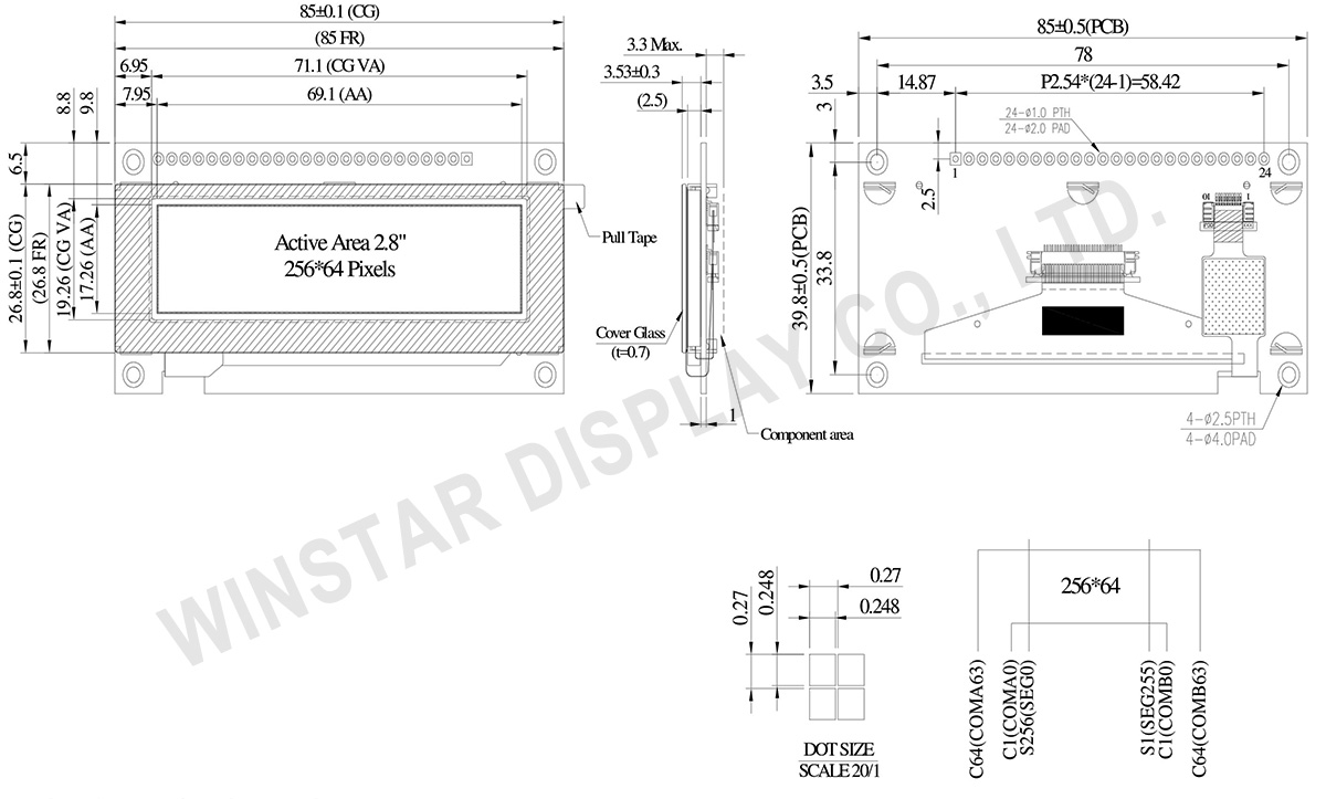
WEN025664A-CTPは、2.8インチのモノクロCOFグラフィックOLEDディスプレイモジュールで、投影型静電容量式タッチパネル(PCAP)を搭載し、256×64ドットの解像度を備えています。コントローラにはSSD1322を採用し、6800/8080系 8ビットパラレルおよび3線/4線SPIインターフェースに対応しています。外形寸法は85.0 × 39.8 mm、表示エリアは69.1 × 17.26 mmです。タッチパネルにはFT6336Uを採用し、I²Cインターフェースおよび1点タッチに対応しています。
本OLEDモジュールは3V電源で動作し、1/64デューティ駆動方式を採用しています。グレースケール表示に対応し、コントラスト比は10,000:1を実現しています。動作温度範囲は-20℃~+70℃、保存温度範囲は-30℃~+80℃です。
WEN025664A-CTPは、金属フレームおよび基板一体構造を採用し、4か所の取付穴を備えることで機構設計への組み込みを容易にします。インターフェースおよびVDD回路が基板上に統合されているため、配線接続によりそのままシステムへ組み込むことができ、システム設計の簡素化や追加基板の削減に寄与します。
WEN025664A-CTPシリーズには、タッチパネル非搭載モデルも用意されています。非タッチ仕様については、WEN025664Aシリーズをご参照ください。
| 項目 | 仕様 | 単位 |
|---|---|---|
| ドットマトリックス | 256 × 64 Dots | - |
| モジュールサイズ | 85.0 × 39.8 ×7.83 | mm |
| アクティブエリア | 69.1 × 17.26 | mm |
| ドットサイズ | 0.248 × 0.248 | mm |
| ドットピッチ | 0.27 × 0.27 | mm |
| 表示モード | パッシブマトリクス | |
| 発光色 | モノクロ | |
| 駆動方法 | 1/64 Duty | |
| OLED IC | SSD1322 (COF) | |
| OLED インターフェイス | 6800, 8080, SPI | |
| 表示サイズ(対角線) | 2.8 インチ | |
| CTP IC | FT6336U | |
| 検出ポイント | 1 | |
| CTP インターフェイス | I2C | |
| 表面処理 | グレア | |
| パラメーター | 記号 | 最小値 | 最大値 | 単位 |
|---|---|---|---|---|
| ディスプレイの供給電圧 | VDD | -0.3 | 4 | V |
| 操作温度 | TOP | -20 | +70 | °C |
| 保存温度 | TSTG | -30 | +80 | °C |
| 項目 | 記号 | 条件 | 最小値 | 典型値 | 最大値 | 単位 |
|---|---|---|---|---|---|---|
| ロジック電源電圧 | VDD | - | 2.8 | 3.0 | 3.3 | V |
| 高レベル入力 | VIH | - | 0.8×VDD | - | VDD | V |
| 低レベル入力 | VIL | - | 0 | - | 0.2×VDD | V |
| 高レベル出力 | VOH | - | 0.9×VDD | - | VDD | V |
| 低レベル出力 | VOL | - | 0 | - | 0.1×VDD | V |
| 50% チェックボード動作電流 | IDD | VDD =3V | - | 125 | 250 | mA |
| Pin Number | 記号 | I/O | 説明 | ||||||||||
|---|---|---|---|---|---|---|---|---|---|---|---|---|---|
| 1 | VSS | P | Ground. | ||||||||||
| 2 | VDD | P | Power Supply for Core Logic Circuit Power supply pin for core logic operation. A capacitor is required to connect between this pin and VSS |
||||||||||
| 3 | N.C. | P | Reserved Pin The N.C. pin between function pins are reserved for compatible and flexible design. |
||||||||||
| 4 | D/C# | I | Data/Command Control This pin is Data/Command control pin connecting to the MCU. When the pin is pulled HIGH, the content at D[7:0] will be interpreted as data. When the pin is pulled LOW, the content at D[7:0] will be interpreted as command. |
||||||||||
| 5 | R/W# (WR#) |
I | Read/Write Select or Write This pin is MCU interface input. When interfacing to a 68XX-series microprocessor, this pin will be used as Read/Write (R/W#) selection input. Pull this pin to “High” for read mode and pull it to “Low” for write mode. When 80XX interface mode is selected, this pin will be the Write (WR#) input. Data write operation is initiated when this pin is pulled low and the CS# is pulled low. When serial mode is selected, this pin must be connected to VSS. |
||||||||||
| 6 | E/RD# | I | Read/Write Enable or Read This pin is MCU interface input. When interfacing to a 68XX-series microprocessor, this pin will be used as the Enable (E) signal. Read/write operation is initiated when this pin is pulled high and the CS# is pulled low. When connecting to an 80XX-microprocessor, this pin receives the Read (RD#) signal. Data read operation is initiated when this pin is pulled low and CS# is pulled low. When serial mode is selected, this pin must be connected to VSS. |
||||||||||
| 7~14 | DB0 | I/O | Host Data Input/Output Bus These pins are 8-bit bi-directional data bus to be connected to the microprocessor’s data bus. When serial mode is selected, D1 will be the serial data input SDIN and D0 will be the serial clock input SCLK. |
||||||||||
| DB1 | |||||||||||||
| DB2 | |||||||||||||
| DB3 | |||||||||||||
| DB4 | |||||||||||||
| DB5 | |||||||||||||
| DB6 | |||||||||||||
| DB7 | |||||||||||||
| 15 | NC | P | Reserved Pin The N.C. pin between function pins are reserved for compatible and flexible design. |
||||||||||
| 16 | RES# | I | This pin is reset signal input. When the pin is pulled LOW, initialization of the chip is executed. Keep this pin pull HIGH during normal operation. |
||||||||||
| 17 | CS# | I | Data/Command Control This pin is the chip select input connecting to the MCU. The chip is enabled for MCU communication only when CS# is pulled LOW. |
||||||||||
| 18 | NC | P | Reserved Pin The N.C. pin between function pins are reserved for compatible and flexible design. |
||||||||||
| 19 | BS1 | I | Communicating Protocol Select These pins are MCU interface selection input. See the following table:
Note (1) 0 is connected to VSS (2) 1 is connected to VDD |
||||||||||
| 20 | BS0 | ||||||||||||
| 21 | TP_SCK | I | I2C clock input | ||||||||||
| 22 | TP_SDA | I | I2C data input and output | ||||||||||
| 23 | TP_INT | I | External interrupt to the host | ||||||||||
| 24 | TP_RST | I | External Reset, Low is active |

「すべてのクッキーを許可」をクリックすると、サイトのナビゲーションを向上させ、サイト使用状況を分析し、マーケティングおよびパフォーマンスの取り組みを支援するために、クッキーをデバイスに保存することに同意したことになります。この件に関する詳細情報は、ポリシーをご覧ください。プライバシーポリシー