
 配备铁框 - WEF012864U")


 - WO160160A")
我们重视您的隐私
通过点击「允许所有 Cookie」,代表您同意在您的设备上存储 Cookie 以增强网站浏览体验、分析网站使用情况并协助我们的营销和网站效能优化工作。您可以在我们的隐私权政策中找到有关于此的更多信息。


WEP012864U-CTP 是一款 COG 绘图型 OLED 显示器模块,采用电容式触控面板,分辨率为 128x64 点,有效区域为 2.7 寸 (61.41 × 30.69 mm) 。 此模块配备SSD1357 IC,支持6800/8080 8位和4线SPI,以及I2C接口。 此显示器支持4位灰度,逻辑电压为3V,占空比为1/64。 电容式触控屏幕内建IC GT911,支持I2C接口与1点触控功能。
WEP012864U-CTP OLED 系列配有金属框架和 PCB 板,可透过电线轻松连接到应用程序。 客户无需自行开发额外的PCB板,整合了接口设定和VCC电路,简化了用户体验。 PCB上设计有四个螺孔,方便模块安装在应用产品上。
此 OLED 模块拥有 10,000:1 的高对比度度,可呈现更鲜艳、更深的黑色以及更明亮的白色。 这可以提高影像质量、更清晰的细节并提高可读性。 模块的工作温度范围为-20℃至70℃,储存温度范围为-30℃至80℃。WEP012864U采用CTP触控屏幕,非常适合智能家庭应用、高科技设备、仪表设备、工业控制系统、医疗仪器等。
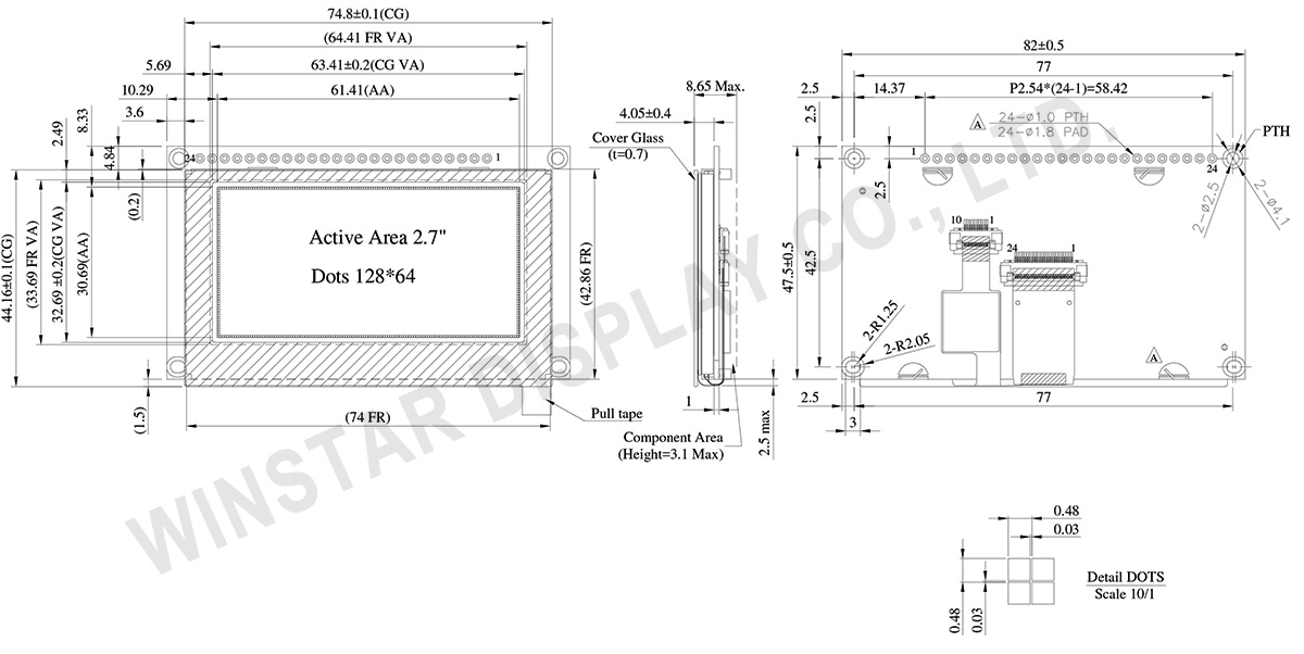
Data source ref: WEP012864UWPP3D00000
| 项目 | 尺寸 | 单位 |
|---|---|---|
| 点阵(分辨率) | 128 x 64 | - |
| 模块尺寸 | 82.0 × 47.5 × 8.65 Max. | mm |
| 有效区域 | 61.41 × 30.69 | mm |
| 点大小 | 0.45 × 0.45 | mm |
| 点间距 | 0.48 × 0.48 | mm |
| 显示模式 | 被动矩阵 | |
| 显示颜色 | 单色 | |
| 驱动方式 | 1/64 Duty | |
| 灰阶 | 4 bits | |
| IC | SSD1357 | |
| 接口 | 8-bits 6800 和 8080 并列, 4线 SPI, I2C | |
| 尺寸 | 2.7 寸 | |
| CTP IC | GT911 |
| 支援手指数 | 1 |
| CTP 接口 | I2C |
| 表面 | 亮面 |
| 参数 | 符号 | 最小值 | 最大值 | 单位 |
|---|---|---|---|---|
| 逻辑电源电压 | VDD | -0.3 | 4.0 | V |
| 工作温度 | TOP | -20 | +70 | °C |
| 储存温度 | TSTG | -30 | +80 | °C |
| 项目 | 符号 | 条件 | 最小值 | 典型值 | 最大值 | 单位 |
|---|---|---|---|---|---|---|
| 逻辑电源电压 | VDD | - | 2.8 | 3.0 | 3.3 | V |
| 输入高准位 | VIH | - | 0.8×VDD | - | - | V |
| 输入低准位 | VIL | - | - | - | 0.2×VDD | V |
| 输出高准位 | VOH | - | 0.9×VDD | - | - | V |
| 输出低准位 | VOL | - | - | - | 0.1×VDD | V |
| 50%显示画面耗电流 | IDD | VDD =3V | - | 160 | 240 | mA |
| No. | 符号 | 功能说明 | |||||||||||||||
|---|---|---|---|---|---|---|---|---|---|---|---|---|---|---|---|---|---|
| 1 | VSS | This is a ground pin. | |||||||||||||||
| 2 | VDD | Power supply pin for core logic operation | |||||||||||||||
| 3 | NC | Reserved Pin The N.C. pin between function pins is reserved for compatible and flexible design. |
|||||||||||||||
| 4 | D/C# | This pin is Data/Command control pin connecting to the MCU. When the pin is pulled HIGH, the data at D[7:0] will be interpreted as data. When the pin is pulled LOW, the data at D[7:0] will be transferred to a command register. In I2C mode, this pin acts as SA0 for slave address selection. When 3-wire serial interface is selected, this pin must be connected to VSS. |
|||||||||||||||
| 5 | R/W# (WR#) |
This pin is read / write control input pin connecting to the MCU interface. When 6800 interface mode is selected, this pin will be used as Read/Write (R/W#) selection input. Read mode will be carried out when this pin is pulled HIGH and write mode when LOW. When 8080 interface mode is selected, this pin will be the Write (WR#) input. Data write operation is initiated when this pin is pulled LOW and the chip is selected. When serial or I2C interface is selected, this pin must be connected to VSS. |
|||||||||||||||
| 6 | E/RD# | This pin is MCU interface input. When 6800 interface mode is selected, this pin will be used as the Enable (E) signal. Read/write operation is initiated when this pin is pulled HIGH and the chip is selected. When 8080 interface mode is selected, this pin receives the Read (RD#) signal. Read operation is initiated when this pin is pulled LOW and the chip is selected. When serial or I2C interface is selected, this pin must be connected to VSS. |
|||||||||||||||
| 7 | DB0 | These pins are bi-directional data bus connecting to the MCU data bus. Unused pins are recommended to tie LOW. When serial interface mode is selected, D0 will be the serial clock input: SCLK; D1 will be the serial data input: SDIN. When I2C mode is selected, D2, D1 should be tied together and serve as SDAout, SDAin in application and D0 is the serial clock input, SCL. |
|||||||||||||||
| 8 | DB1 | ||||||||||||||||
| 9 | DB2 | ||||||||||||||||
| 10 | DB3 | ||||||||||||||||
| 11 | DB4 | ||||||||||||||||
| 12 | DB5 | ||||||||||||||||
| 13 | DB6 | ||||||||||||||||
| 14 | DB7 | ||||||||||||||||
| 15 | NC | No connection | |||||||||||||||
| 16 | RES# | This pin is reset signal input. When the pin is pulled LOW, initialization of the chip is executed. Keep this pin pull HIGH during normal operation. |
|||||||||||||||
| 17 | CS# | Chip Select This pin is the chip select input. The chip is enabled for MCU communication only when CS# is pulled low. |
|||||||||||||||
| 18 | NC | No connection | |||||||||||||||
| 19 | BS2 | Communicating Protocol Select. These pins are MCU interface selection input. See the following table:
|
|||||||||||||||
| 20 | BS1 | ||||||||||||||||
| 21 | TP_SCK | I2C clock signal | |||||||||||||||
| 22 | TP_SDA | I2C data signal | |||||||||||||||
| 23 | TP_INT | Interrupt signal, active low, asserted to request Host start a new transaction |
|||||||||||||||
| 24 | TP_RST | External reset signal, active low |

通过点击「允许所有 Cookie」,代表您同意在您的设备上存储 Cookie 以增强网站浏览体验、分析网站使用情况并协助我们的营销和网站效能优化工作。您可以在我们的隐私权政策中找到有关于此的更多信息。