Home Produtos Display OLED Display OLED Tátil WEP012864U-CTP

Display OLED 128x64 de 2,7 polegadas com Painel Tátil Capacitivo

Model No. WEP012864U-CTP

►Tipo: Gráfico
►Estrutura: COG + Frame + PCB
►Tamanho: 2,7 polegadas
►Matriz de pontos 128 x 64
►IC:SSD1357
►Alimentação 3V
►1/64 duty
►Interface: 6800, 8080, SPI, I2C
►Tela de Toque: Com painel de toque capacitivo (CTP)
►Detect Point : 1 Finger
►Display Color: Branco / Amarelo
►Support Grayscale

Descrição

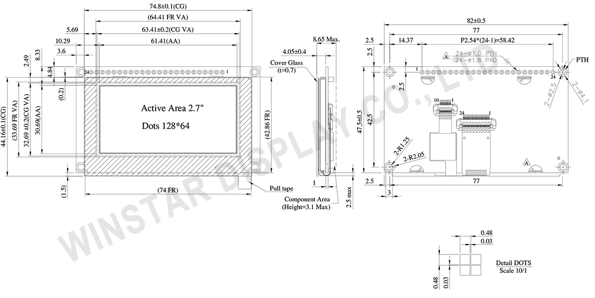
WEP012864U-CTP é um ecrã OLED gráfico COG com um painel tátil capacitivo, com uma resolução de 128x64 pixels e uma área ativa de 2,7 polegadas (61,41 x 30,69 mm). O circuito integrado SSD1357 deste módulo suporta interfaces de 6800/8080 de 8 bits e SPI de 4 fios, bem como a interface I2C. O ecrã suporta 4 bits de escala de cinzentos, com uma tensão lógica de 3V e um ciclo de serviço de 1/64. O painel tátil capacitivo inclui o circuito integrado GT911, suportando uma interface I2C com capacidade de toque de um ponto.

A série OLED WEP012864U-CTP possui uma estrutura metálica e uma placa de circuito impresso que se conecta facilmente à aplicação através de fios. Os clientes não precisam desenvolver placas de circuito impresso adicionais por si próprios. Integra definições de interface e circuitos VCC, tornando a sua utilização fácil para os clientes. Quatro furos roscados são concebidos na placa de circuito impresso para facilitar a instalação do módulo no produto de aplicação.

Este módulo OLED apresenta uma elevada relação de contraste de 10.000:1, o que permite pretos mais vibrantes e profundos, bem como brancos mais brilhantes. Isto resulta numa qualidade de imagem melhorada, detalhes mais nítidos e uma legibilidade melhorada. O módulo pode operar numa gama de temperaturas de -20°C a 70°C, com temperaturas de armazenamento que variam de -30°C a 80°C.

O WEP012864U com o painel tátil CTP é muito adequado para aplicações domóticas, equipamentos de alta tecnologia, equipamentos de medição, sistemas de controlo industrial, instrumentos médicos, etc.

DRAWING

WEP012864U-CTP
 

Data source ref: WEP012864UWPP3D00000

SPECIFICATIONS

Função do pino de interface

No. Símbolo Função
1 VSS This is a ground pin.
2 VDD Power supply pin for core logic operation
3 NC Reserved Pin
The N.C. pin between function pins is reserved for compatible and flexible design.
4 D/C# This pin is Data/Command control pin connecting to the MCU.
When the pin is pulled HIGH, the data at D[7:0] will be interpreted as data.
When the pin is pulled LOW, the data at D[7:0] will be transferred to a command register.
In I2C mode, this pin acts as SA0 for slave address selection.
When 3-wire serial interface is selected, this pin must be connected to VSS.
5 R/W#
(WR#)
This pin is read / write control input pin connecting to the MCU interface.
When 6800 interface mode is selected, this pin will be used as Read/Write (R/W#) selection input. Read mode will be carried out when this pin is pulled HIGH and write mode when LOW.
When 8080 interface mode is selected, this pin will be the Write (WR#) input. Data write operation is initiated when this pin is pulled LOW and the chip is selected.
When serial or I2C interface is selected, this pin must be connected to VSS.
6 E/RD# This pin is MCU interface input.
When 6800 interface mode is selected, this pin will be used as the Enable (E) signal.
Read/write operation is initiated when this pin is pulled HIGH and the chip is selected.
When 8080 interface mode is selected, this pin receives the Read (RD#) signal. Read operation is initiated when this pin is pulled LOW and the chip is selected.
When serial or I2C interface is selected, this pin must be connected to VSS.
7 DB0 These pins are bi-directional data bus connecting to the MCU data bus.
Unused pins are recommended to tie LOW.
When serial interface mode is selected, D0 will be the serial clock input: SCLK; D1 will be the serial data input: SDIN.
When I2C mode is selected, D2, D1 should be tied together and serve as SDAout, SDAin in application and D0 is the serial clock input, SCL.
8 DB1
9 DB2
10 DB3
11 DB4
12 DB5
13 DB6
14 DB7
15 NC No connection
16 RES# This pin is reset signal input.
When the pin is pulled LOW, initialization of the chip is executed.
Keep this pin pull HIGH during normal operation.
17 CS# Chip Select
This pin is the chip select input. The chip is enabled for MCU communication only when CS# is pulled low.
18 NC No connection
19 BS2 Communicating Protocol Select.
These pins are MCU interface selection input. See the following table:
  BS1 BS2
I2C 1 0
4-wire Serial 0 0
8-bit 8080 Parallel 1 1
8-bit 6800 Parallel 0 1
20 BS1
21 TP_SCK I2C clock signal
22 TP_SDA I2C data signal
23 TP_INT Interrupt signal, active low, asserted to request
Host start a new transaction
24 TP_RST External reset signal, active low

Dados Mecânicos

Item Dimensão Unidade
Matriz de pontos 128 x 64
Dimensão do módulo 82.0 × 47.5 × 8.65 Max. mm
Área ativa 61.41 × 30.69 mm
Tamanho do ponto 0.45 × 0.45 mm
Distância entre pontos 0.48 × 0.48 mm
Modo de exibição Passive Matrix
Cor de exibição Monochrome
Drive Duty 1/64 Duty
Gray Scale 4 bits
IC SSD1357
Interface 8-bits 6800 and 8080 parallel, 4-line SPI, I2C
Tamanho 2,7 polegadas
 
CTP IC GT911
Detect Point 1
CTP Interface I2C
Superfície Reflexo

Classificações Máximas Absolutas

Parameter Símbolo Valor Min Valor Máximo Unidade
Supply Voltage for Logic VDD -0.3 4.0 V
Temperatura de operação TOP -20 +70 °C
Temperatura de armazenamento TSTG -30 +80 °C
 

Características Eletrônicas

DC Características Eletrônicas

Item Símbolo Condição Valor Min Valor Típico Valor Máximo Unidade
Supply Voltage for Logic VDD 2.8 3.0 3.3 V
High Level Input VIH 0.8×VDD V
Low Level Input VIL 0.2×VDD V
High Level Output VOH 0.9×VDD V
Low Level Output VOL 0.1×VDD V
50% Check Board operating Current IDD VDD =3V 160 240 mA
go top
close