Home Produtos Display OLED Display OLED Gráfico WEP012864U

Display OLED COG de 2,7 polegadas, 128x64, suporte a tons de cinza, com PCB e estrutura.

Model No. WEP012864U

►Tipo: Gráfico
►Estrutura: COG + Frame + PCB
►Tamanho: 2,7 polegadas
►Matriz de pontos 128 x 64
►IC:SSD1357
►Alimentação 3V
►1/64 duty
►Interface: 6800, 8080, SPI, I2C
►Display Color: Branco / Amarelo
►Support Grayscale

Descrição

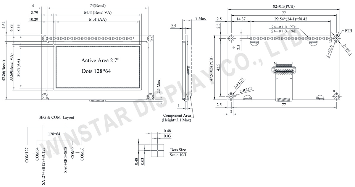
O WEP012864U é um ecrã OLED gráfico com uma estrutura COG, uma resolução de 128x64 pontos e uma área ativa de 2,7 polegadas (61,41 × 30,69 mm). O módulo está equipado com o circuito integrado SSD1357, suportando interfaces 6800/8080 de 8 bits, 4 fios SPI e interfaces I2C. O ecrã suporta escala de cinzentos de 4 bits, com uma voltagem lógica de 3V e um ciclo de trabalho de 1/64.

A série OLED WEP012864U vem com uma estrutura metálica e uma placa de circuito impresso (PCB) que se conecta facilmente à aplicação por meio de fios. Os clientes não precisam desenvolver placas de circuito impresso adicionais, pois ela integra configurações de interface e circuitos VCC, simplificando a experiência do utilizador. A PCB é projetada com quatro orifícios de parafuso para facilitar a instalação do módulo no produto de aplicação.

Este módulo OLED possui uma taxa de contraste elevada de 10.000:1, permitindo pretos mais vibrantes e profundos, assim como brancos mais brilhantes. Isso resulta em uma qualidade de imagem aprimorada, detalhes mais nítidos e melhor legibilidade. O módulo é operacional numa faixa de temperatura de -40℃ a 80℃, com temperaturas de armazenamento variando de -40℃ a 85℃.

É ideal para dispositivos de parede/medidores, aplicações residenciais, sistemas financeiros POS, sistemas Cloud/IoT, dispositivos de tecnologia inteligente, sistemas de energia, sistemas de comunicação, instrumentos médicos, etc.

Além disso, painéis OLED semelhantes estão disponíveis na série WEO012864U sem estrutura metálica e PCB, e na série WEF012864U com estrutura metálica, mas sem PCB. Se você tiver requisitos de funcionalidade de toque, considere a série WEP012864U-CTP.

DRAWING

WEP012864U

Data source ref:WEP012864ULAP3N00000

SPECIFICATIONS

Função do pino de interface

No. Símbolo Função
1 VSS This is a ground pin.
2 VDD Power supply pin for core logic operation
3 NC Reserved Pin
The N.C. pin between function pins is reserved for compatible and flexible design.
4 D/C# This pin is Data/Command control pin connecting to the MCU.
When the pin is pulled HIGH, the data at D[7:0] will be interpreted as data.
When the pin is pulled LOW, the data at D[7:0] will be transferred to a command register.
In I2C mode, this pin acts as SA0 for slave address selection.
5 R/W#
(WR#)
This pin is read / write control input pin connecting to the MCU interface.
When 6800 interface mode is selected, this pin will be used as Read/Write (R/W#) selection input. Read mode will be carried out when this pin is pulled HIGH and write mode when LOW.
When 8080 interface mode is selected, this pin will be the Write (WR#) input. Data write operation is initiated when this pin is pulled LOW and the chip is selected.
When serial or I2C interface is selected, this pin must be connected to VSS.
6 E/RD# This pin is MCU interface input.
When 6800 interface mode is selected, this pin will be used as the Enable (E) signal.
Read/write operation is initiated when this pin is pulled HIGH and the chip is selected.
When 8080 interface mode is selected, this pin receives the Read (RD#) signal. Read operation is initiated when this pin is pulled LOW and the chip is selected.
When serial or I2C interface is selected, this pin must be connected to VSS.
7 DB0 These pins are bi-directional data bus connecting to the MCU data bus.
Unused pins are recommended to tie LOW.
When serial interface mode is selected, D0 will be the serial clock input: SCLK; D1 will be the serial data input: SDIN.
When I2C mode is selected, D2, D1 should be tied together and serve as SDAout, SDAin in application and D0 is the serial clock input, SCL.
8 DB1
9 DB2
10 DB3
11 DB4
12 DB5
13 DB6
14 DB7

15
NC No connection.
16 RES# This pin is reset signal input.
When the pin is pulled LOW, initialization of the chip is executed.
Keep this pin pull HIGH during normal operation.

17
CS# Chip Select
This pin is the chip select input. The chip is enabled for MCU communication only when CS# is pulled low.
18 NC No connection.
19 BS2 Communicating Protocol Select.
These pins are MCU interface selection input. See the following table:
  BS1 BS2
I2C 1 0
4-wire Serial 0 0
8-bit 8080 Parallel 1 1
8-bit 6800 Parallel 0 1
20 BS1
21 NC No connection.
22 NC No connection.
23 NC No connection.
24 NC No connection.

Dados Mecânicos

Item Dimensão Unidade
Matriz de pontos 128 x 64 Pontos
Dimensão do módulo 82.0 × 47.5 × 7 Max. mm
Área ativa 61.41 × 30.69 mm
Tamanho do ponto 0.45 × 0.45 mm
Distância entre pontos 0.48 × 0.48 mm
Modo de exibição Passive Matrix
Cor de exibição Monochrome
Drive Duty 1/64 Duty
Gray Scale 4 bits
IC SSD1357
Interface 6800, 8080, SPI, I2C
Tamanho 2,7 polegadas

Classificações Máximas Absolutas

Parameter Símbolo Valor Min Valor Máximo Unidade
Supply Voltage for Logic VDD -0.3 4.0 V
Temperatura de operação TOP -40 80 °C
Temperatura de armazenamento TSTG -40 85 °C

Características Eletrônicas

Item Símbolo Condição Valor Min Valor Típico Valor Máximo Unidade
Supply Voltage for Logic VDD 2.8 3.0 3.3 V
High Level Input VIH 0.8×VDD V
Low Level Input VIL 0.2×VDD V
High Level Output VOH 0.9×VDD V
Low Level Output VOL 0.1×VDD V
Display 50% Pixel on IDD VDD =3V 120 180 mA
go top
close