2,7-Zoll 128x64 COG OLED-Display mit PCB und Rahmen, Unterstützung für Graustufen
Modellnummer WEP012864U
►Typ: Grafik
►Bauweise: COG + Frame + PCB
►Größe: 2,7 Zoll
►128 x 64 Punktmatrix
►IC:SSD1357
►3-V-Stromversorgung
►1/64 duty
►Schnittstelle: 6800, 8080, SPI, I2C
►die Farbe des Displays: Weiß / Gelb
►Unterstützt Grauskala
Beschreibung
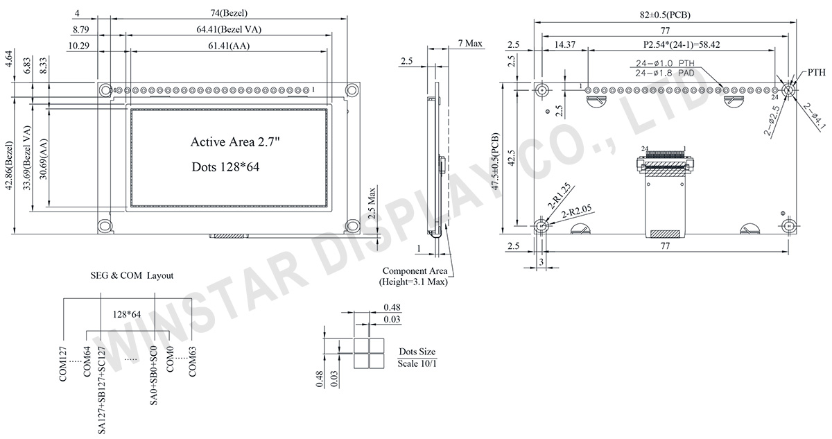
Der WEP012864U ist ein grafischer OLED-Bildschirm mit COG-Struktur und einer Auflösung von 128x64 Punkten auf einer aktiven Fläche von 2,7 Zoll (61,41 × 30,69 mm). Das Modul ist mit dem SSD1357-IC ausgestattet und unterstützt 6800/8080 8-Bit sowie 4-Draht-SPI- und I2C-Schnittstellen. Der Bildschirm unterstützt 4-Bit- Graustufen, mit einer Logikspannung von 3V und einer Tastverhältnis von 1/64.
Die OLED-Serie WEP012864U wird mit einem Metallrahmen und einer Leiterplatte (PCB) geliefert, die über Drähte leicht mit der Anwendung verbunden werden kann. Kunden müssen keine zusätzlichen Leiterplatten selbst entwickeln, da sie Interface-Einstellungen und VCC-Schaltungen integriert, was die Benutzererfahrung vereinfacht. Die Leiterplatte ist mit vier Schraubenlöchern für eine einfache Installation des Moduls auf dem Anwendungsprodukt ausgelegt.
Dieses OLED-Modul verfügt über ein hohes Kontrastverhältnis von 10.000:1, was lebendigere und tiefere Schwarztöne sowie hellere Weißtöne ermöglicht. Dies führt zu einer verbesserten Bildqualität, schärferen Details und verbesserter Lesbarkeit. Das Modul ist im Temperaturbereich von -40℃ bis 80℃ betriebsbereit, mit Lagerungstemperaturen von -40℃ bis 85℃.
Es eignet sich ideal für Wand-/Messgeräte, Anwendungen im Haushalt, Finanz-POS, Cloud/IoT-Systeme, intelligente Technologiegeräte, Energiesysteme, Kommunikationssysteme, medizinische Instrumente, etc.
Zusätzlich sind ähnliche OLED-Panels in der Serie WEO012864U ohne Metallrahmen und PCB sowie in der Serie WEF012864U mit Metallrahmen, aber ohne PCB erhältlich. Wenn Sie Touch-Funktionalität benötigen, sollten Sie die Serie WEP012864U-CTP in Betracht ziehen.
Zeichnung
Data source ref:WEP012864ULAP3N00000
Technische Daten
Schnittstelle Pin-Funktion
No. | Symbol | Funktion | |||||||||||||||
---|---|---|---|---|---|---|---|---|---|---|---|---|---|---|---|---|---|
1 | VSS | This is a ground pin. | |||||||||||||||
2 | VDD | Power supply pin for core logic operation | |||||||||||||||
3 | NC | Reserved Pin The N.C. pin between function pins is reserved for compatible and flexible design. |
|||||||||||||||
4 | D/C# | This pin is Data/Command control pin connecting to the MCU. When the pin is pulled HIGH, the data at D[7:0] will be interpreted as data. When the pin is pulled LOW, the data at D[7:0] will be transferred to a command register. In I2C mode, this pin acts as SA0 for slave address selection. |
|||||||||||||||
5 | R/W# (WR#) |
This pin is read / write control input pin connecting to the MCU interface. When 6800 interface mode is selected, this pin will be used as Read/Write (R/W#) selection input. Read mode will be carried out when this pin is pulled HIGH and write mode when LOW. When 8080 interface mode is selected, this pin will be the Write (WR#) input. Data write operation is initiated when this pin is pulled LOW and the chip is selected. When serial or I2C interface is selected, this pin must be connected to VSS. |
|||||||||||||||
6 | E/RD# | This pin is MCU interface input. When 6800 interface mode is selected, this pin will be used as the Enable (E) signal. Read/write operation is initiated when this pin is pulled HIGH and the chip is selected. When 8080 interface mode is selected, this pin receives the Read (RD#) signal. Read operation is initiated when this pin is pulled LOW and the chip is selected. When serial or I2C interface is selected, this pin must be connected to VSS. |
|||||||||||||||
7 | DB0 | These pins are bi-directional data bus connecting to the MCU data bus. Unused pins are recommended to tie LOW. When serial interface mode is selected, D0 will be the serial clock input: SCLK; D1 will be the serial data input: SDIN. When I2C mode is selected, D2, D1 should be tied together and serve as SDAout, SDAin in application and D0 is the serial clock input, SCL. |
|||||||||||||||
8 | DB1 | ||||||||||||||||
9 | DB2 | ||||||||||||||||
10 | DB3 | ||||||||||||||||
11 | DB4 | ||||||||||||||||
12 | DB5 | ||||||||||||||||
13 | DB6 | ||||||||||||||||
14 | DB7 | ||||||||||||||||
15 |
NC | No connection. | |||||||||||||||
16 | RES# | This pin is reset signal input. When the pin is pulled LOW, initialization of the chip is executed. Keep this pin pull HIGH during normal operation. |
|||||||||||||||
17 |
CS# | Chip Select This pin is the chip select input. The chip is enabled for MCU communication only when CS# is pulled low. |
|||||||||||||||
18 | NC | No connection. | |||||||||||||||
19 | BS2 | Communicating Protocol Select. These pins are MCU interface selection input. See the following table:
|
|||||||||||||||
20 | BS1 | ||||||||||||||||
21 | NC | No connection. | |||||||||||||||
22 | NC | No connection. | |||||||||||||||
23 | NC | No connection. | |||||||||||||||
24 | NC | No connection. |
mechanische Daten
Artikel | Ausmaß | Einheit |
---|---|---|
Punktmatrix | 128 x 64 | Punkte |
Abmaße der modul | 82,0 × 47,5 × 7 Max. | mm |
Aktiver Bereich | 61,41 × 30,69 | mm |
Pixelgröße | 0,45 × 0,45 | mm |
Pixelabstand | 0,48 × 0,48 | mm |
der Anzeigemodus | Passive Matrix | |
die Farbe des Displays | Monochrome | |
Drive Duty | 1/64 Duty | |
Gray-Scale | 4 bits | |
IC | SSD1357 | |
Schnittstelle | 6800, 8080, SPI, I2C | |
Größe | 2,7 Zoll |
absolute Grenzwerte
Parameter | Symbol | Mindestwert | Maximalwert | Einheit |
---|---|---|---|---|
Supply Voltage for Logic | VDD | -0,3 | 4.0 | V |
Betriebstemperatur | TOP | -40 | 80 | °C |
Lagertemperatur | TSTG | -40 | 85 | °C |
elektronische Eingenschaften
Artikel | Symbol | Bedingung | Mindestwert | typischer Wert | Maximalwert | Einheit |
---|---|---|---|---|---|---|
Supply Voltage for Logic | VDD | - | 2,8 | 3,0 | 3,3 | V |
High Level Input | VIH | - | 0,8×VDD | - | - | V |
Low Level Input | VIL | - | - | - | 0,2×VDD | V |
High Level Output | VOH | - | 0,9×VDD | - | - | V |
Low Level Output | VOL | - | - | - | 0,1×VDD | V |
Display 50% Pixel on | IDD | VDD =3V | - | 120 | 180 | mA |