Pantalla OLED COG de 2.7 pulgadas, 128x64, compatible con tonos de gris, con PCB y marco
Modelo Nº WEP012864U
►Tipo : Gráfico
►Estructura : COG + marco + PCB
►Tamaño : 2.7 pulgada
►Matriz de puntos 128 x 64
►IC:SSD1357
►Fuente de alimentación de 3V
►1/64 duty
►Interfaz : 6800, 8080, SPI, I2C
►Color de la pantalla: Blanco / Amarillo
►Compatibilidad con escala de grises
Descripción
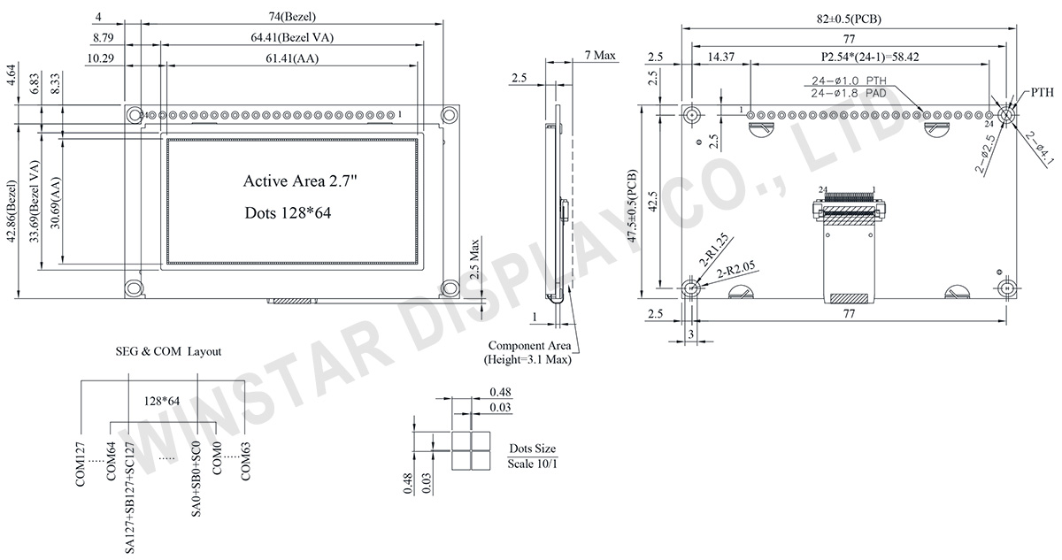
El WEP012864U es una pantalla OLED gráfica con una estructura COG y una resolución de 128x64 puntos en un área activa de 2.7 pulgadas (61.41 × 30.69 mm). El módulo está equipado con el circuito integrado SSD1357, compatible con interfaces 6800/8080 de 8 bits y 4 hilos SPI, así como interfaces I2C. La pantalla admite grises de 4 bits, con un voltaje lógico de 3V y un ciclo de trabajo de 1/64.
La serie OLED WEP012864U viene con un marco metálico y una placa de circuito impreso (PCB) que se conecta fácilmente a la aplicación mediante cables. No es necesario que los clientes desarrollen placas de circuito impreso adicionales, ya que integra configuraciones de interfaz y circuitos VCC, simplificando la experiencia del usuario. La PCB está diseñada con cuatro agujeros para tornillos para facilitar la instalación del módulo en el producto de aplicación.
Este módulo OLED presume una alta relación de contraste de 10,000:1, lo que permite negros más vibrantes y profundos, así como blancos más brillantes. Esto se traduce en una calidad de imagen mejorada, detalles más nítidos y una mejor legibilidad. El módulo es operativo en un rango de temperatura de -40℃ a 80℃, con temperaturas de almacenamiento que van desde -40℃ a 85℃.
Es ideal para dispositivos de pared/medidores, aplicaciones domésticas, sistemas financieros POS, sistemas Cloud/IoT, dispositivos de tecnología inteligente, sistemas de energía, sistemas de comunicación, instrumentos médicos, etc.
Además, paneles OLED similares están disponibles en la serie WEO012864U sin marco metálico y PCB, y la serie WEF012864U con un marco metálico pero sin PCB. Si tiene requisitos de funcionalidad táctil, considere la serie WEP012864U-CTP.
DIBUJO
Data source ref:WEP012864ULAP3N00000
ESPECIFICACIONES
Función interfaz Pin
No. | Símbolo | Función | |||||||||||||||
---|---|---|---|---|---|---|---|---|---|---|---|---|---|---|---|---|---|
1 | VSS | This is a ground pin. | |||||||||||||||
2 | VDD | Power supply pin for core logic operation | |||||||||||||||
3 | NC | Reserved Pin The N.C. pin between function pins is reserved for compatible and flexible design. |
|||||||||||||||
4 | D/C# | This pin is Data/Command control pin connecting to the MCU. When the pin is pulled HIGH, the data at D[7:0] will be interpreted as data. When the pin is pulled LOW, the data at D[7:0] will be transferred to a command register. In I2C mode, this pin acts as SA0 for slave address selection. |
|||||||||||||||
5 | R/W# (WR#) |
This pin is read / write control input pin connecting to the MCU interface. When 6800 interface mode is selected, this pin will be used as Read/Write (R/W#) selection input. Read mode will be carried out when this pin is pulled HIGH and write mode when LOW. When 8080 interface mode is selected, this pin will be the Write (WR#) input. Data write operation is initiated when this pin is pulled LOW and the chip is selected. When serial or I2C interface is selected, this pin must be connected to VSS. |
|||||||||||||||
6 | E/RD# | This pin is MCU interface input. When 6800 interface mode is selected, this pin will be used as the Enable (E) signal. Read/write operation is initiated when this pin is pulled HIGH and the chip is selected. When 8080 interface mode is selected, this pin receives the Read (RD#) signal. Read operation is initiated when this pin is pulled LOW and the chip is selected. When serial or I2C interface is selected, this pin must be connected to VSS. |
|||||||||||||||
7 | DB0 | These pins are bi-directional data bus connecting to the MCU data bus. Unused pins are recommended to tie LOW. When serial interface mode is selected, D0 will be the serial clock input: SCLK; D1 will be the serial data input: SDIN. When I2C mode is selected, D2, D1 should be tied together and serve as SDAout, SDAin in application and D0 is the serial clock input, SCL. |
|||||||||||||||
8 | DB1 | ||||||||||||||||
9 | DB2 | ||||||||||||||||
10 | DB3 | ||||||||||||||||
11 | DB4 | ||||||||||||||||
12 | DB5 | ||||||||||||||||
13 | DB6 | ||||||||||||||||
14 | DB7 | ||||||||||||||||
15 |
NC | No connection. | |||||||||||||||
16 | RES# | This pin is reset signal input. When the pin is pulled LOW, initialization of the chip is executed. Keep this pin pull HIGH during normal operation. |
|||||||||||||||
17 |
CS# | Chip Select This pin is the chip select input. The chip is enabled for MCU communication only when CS# is pulled low. |
|||||||||||||||
18 | NC | No connection. | |||||||||||||||
19 | BS2 | Communicating Protocol Select. These pins are MCU interface selection input. See the following table:
|
|||||||||||||||
20 | BS1 | ||||||||||||||||
21 | NC | No connection. | |||||||||||||||
22 | NC | No connection. | |||||||||||||||
23 | NC | No connection. | |||||||||||||||
24 | NC | No connection. |
Datos mecánicos
Elemento | Dimensión | Unidad |
---|---|---|
Matriz de puntos | 128 x 64 | Dots |
Dimensión del módulo | 82.0 × 47.5 × 7 Max. | mm |
zona activa | 61.41 × 30.69 | mm |
Tamaño del punto | 0.45 × 0.45 | mm |
Distancia entre puntos | 0.48 × 0.48 | mm |
Modo de visualización | Matriz pasiva | |
Color de la pantalla | Monocromos | |
Drive Duty | 1/64 Duty | |
グレースケール | 4 bits | |
IC | SSD1357 | |
Interfaz | 6800, 8080, SPI, I2C | |
Tamaño | 2.7 pulgada |
Valores nominales máximos absolutos
Parameter | Símbolo | Valor mín. | Valor máx. | Unidad |
---|---|---|---|---|
Supply Voltage for Logic | VDD | -0.3 | 4.0 | V |
Temperatura de funcionamiento | TOP | -40 | 80 | °C |
Temperatura de almacenamiento | TSTG | -40 | 85 | °C |
Características electrónicas
Elemento | Símbolo | Condición | Valor mín. | Valor típico | Valor máx. | Unidad |
---|---|---|---|---|---|---|
Supply Voltage for Logic | VDD | - | 2.8 | 3.0 | 3.3 | V |
High Level Input | VIH | - | 0.8×VDD | - | - | V |
Low Level Input | VIL | - | - | - | 0.2×VDD | V |
High Level Output | VOH | - | 0.9×VDD | - | - | V |
Low Level Output | VOL | - | - | - | 0.1×VDD | V |
Display 50% Pixel on | IDD | VDD =3V | - | 120 | 180 | mA |