
- WEO012864U")
 - WEF012864U")
私たちはあなたのプライバシーを大切にします
「すべてのクッキーを許可」をクリックすると、サイトのナビゲーションを向上させ、サイト使用状況を分析し、マーケティングおよびパフォーマンスの取り組みを支援するために、クッキーをデバイスに保存することに同意したことになります。この件に関する詳細情報は、ポリシーをご覧ください。プライバシーポリシー


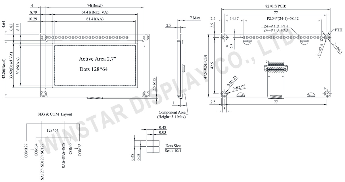
WEP012864Uは、COG構造を採用したグラフィックOLEDディスプレイで、解像度は128x64ドットで、アクティブエリアは2.7インチ(61.41 × 30.69 mm)です。モジュールにはSSD1357 ICが搭載されており、6800/8080 8ビットおよび4線SPI、およびI2Cインターフェースをサポートしています。ディスプレイは4ビットのグレースケールをサポートし、論理電圧は3Vで、デューティサイクルは1/64です。
WEP012864U OLEDシリーズには、ワイヤーを介してアプリケーションに簡単に接続できる金属フレームとPCBボードが付属しています。顧客はPCBボードを追加で開発する必要はありません。インターフェース設定とVCC回路が統合されており、ユーザーエクスペリエンスが簡素化されています。PCBにはアプリケーション製品へのモジュールの簡単な取り付けを可能にする4つのネジ穴が設計されています。
このOLEDモジュールは、10,000:1という高いコントラスト比を誇り、より鮮やかで深いブラック、明るいホワイトを実現します。これにより、向上した画質、より鮮明なディテール、改善された可読性が得られます。モジュールは-40℃から80℃の温度範囲で動作し、-40℃から85℃の温度で保管できます。
壁/計器機器、家庭用アプリケーション、金融POS、クラウド/ IoTシステム、インテリジェントテクノロジー機器、エネルギーシステム、通信システム、医療機器等に最適です。
さらに、WEO012864Uシリーズには金属フレームとPCBのない類似のOLEDパネルがあり、WEF012864Uシリーズには金属フレームがありますがPCBがないものもあります。タッチ機能の要件がある場合は、WEP012864U-CTPシリーズをご検討ください。
| 項目 | 仕様 | 単位 |
|---|---|---|
| ドットマトリックス(解像度) | 128 x 64 | Dots |
| 外形寸法 | 82.0 × 47.5 × 7 Max. | mm |
| 有効表示エリア | 61.41 × 30.69 | mm |
| ドットサイズ | 0.45 × 0.45 | mm |
| ドットピッチ | 0.48 × 0.48 | mm |
| 表示モード | パッシブマトリクス | |
| 発光色 | モノクロ | |
| 駆動方法 | 1/64 Duty | |
| グレースケール | 4 bits | |
| IC | SSD1357 | |
| インターフェイス | 8-bits 6800, 8080 parallel, 4-Wire SPI, I2C | |
| サイズ | 2.7 インチ | |
| パラメーター | 記号 | 最小値 | 最大値 | 単位 |
|---|---|---|---|---|
| ロジック電源電圧 | VDD | -0.3 | 4.0 | V |
| 操作温度 | TOP | -40 | 80 | °C |
| 保存温度 | TSTG | -40 | 85 | °C |
| 項目 | 記号 | 条件 | 最小値 | 典型値 | 最大値 | 単位 |
|---|---|---|---|---|---|---|
| ロジック電源電圧 | VDD | - | 2.8 | 3.0 | 3.3 | V |
| 入力電圧(High) | VIH | - | 0.8×VDD | - | - | V |
| 入力電圧(Low) | VIL | - | - | - | 0.2×VDD | V |
| 出力電圧(High) | VOH | - | 0.9×VDD | - | - | V |
| 出力電圧(Low) | VOL | - | - | - | 0.1×VDD | V |
| Display 50% Pixel on | IDD | VDD =3V | - | 120 | 180 | mA |
| No. | 記号 | 説明 | |||||||||||||||
|---|---|---|---|---|---|---|---|---|---|---|---|---|---|---|---|---|---|
| 1 | VSS | This is a ground pin. | |||||||||||||||
| 2 | VDD | Power supply pin for core logic operation | |||||||||||||||
| 3 | NC | Reserved Pin The N.C. pin between function pins is reserved for compatible and flexible design. |
|||||||||||||||
| 4 | D/C# | This pin is Data/Command control pin connecting to the MCU. When the pin is pulled HIGH, the data at D[7:0] will be interpreted as data. When the pin is pulled LOW, the data at D[7:0] will be transferred to a command register. In I2C mode, this pin acts as SA0 for slave address selection. |
|||||||||||||||
| 5 | R/W# (WR#) |
This pin is read / write control input pin connecting to the MCU interface. When 6800 interface mode is selected, this pin will be used as Read/Write (R/W#) selection input. Read mode will be carried out when this pin is pulled HIGH and write mode when LOW. When 8080 interface mode is selected, this pin will be the Write (WR#) input. Data write operation is initiated when this pin is pulled LOW and the chip is selected. When serial or I2C interface is selected, this pin must be connected to VSS. |
|||||||||||||||
| 6 | E/RD# | This pin is MCU interface input. When 6800 interface mode is selected, this pin will be used as the Enable (E) signal. Read/write operation is initiated when this pin is pulled HIGH and the chip is selected. When 8080 interface mode is selected, this pin receives the Read (RD#) signal. Read operation is initiated when this pin is pulled LOW and the chip is selected. When serial or I2C interface is selected, this pin must be connected to VSS. |
|||||||||||||||
| 7 | DB0 | These pins are bi-directional data bus connecting to the MCU data bus. Unused pins are recommended to tie LOW. When serial interface mode is selected, D0 will be the serial clock input: SCLK; D1 will be the serial data input: SDIN. When I2C mode is selected, D2, D1 should be tied together and serve as SDAout, SDAin in application and D0 is the serial clock input, SCL. |
|||||||||||||||
| 8 | DB1 | ||||||||||||||||
| 9 | DB2 | ||||||||||||||||
| 10 | DB3 | ||||||||||||||||
| 11 | DB4 | ||||||||||||||||
| 12 | DB5 | ||||||||||||||||
| 13 | DB6 | ||||||||||||||||
| 14 | DB7 | ||||||||||||||||
15 |
NC | No connection. | |||||||||||||||
| 16 | RES# | This pin is reset signal input. When the pin is pulled LOW, initialization of the chip is executed. Keep this pin pull HIGH during normal operation. |
|||||||||||||||
17 |
CS# | Chip Select This pin is the chip select input. The chip is enabled for MCU communication only when CS# is pulled low. |
|||||||||||||||
| 18 | NC | No connection. | |||||||||||||||
| 19 | BS2 | Communicating Protocol Select. These pins are MCU interface selection input. See the following table:
|
|||||||||||||||
| 20 | BS1 | ||||||||||||||||
| 21 | NC | No connection. | |||||||||||||||
| 22 | NC | No connection. | |||||||||||||||
| 23 | NC | No connection. | |||||||||||||||
| 24 | NC | No connection. | |||||||||||||||

「すべてのクッキーを許可」をクリックすると、サイトのナビゲーションを向上させ、サイト使用状況を分析し、マーケティングおよびパフォーマンスの取り組みを支援するために、クッキーをデバイスに保存することに同意したことになります。この件に関する詳細情報は、ポリシーをご覧ください。プライバシーポリシー