私たちはあなたのプライバシーを大切にします
「すべてのクッキーを許可」をクリックすると、サイトのナビゲーションを向上させ、サイト使用状況を分析し、マーケティングおよびパフォーマンスの取り組みを支援するために、クッキーをデバイスに保存することに同意したことになります。この件に関する詳細情報は、ポリシーをご覧ください。プライバシーポリシー


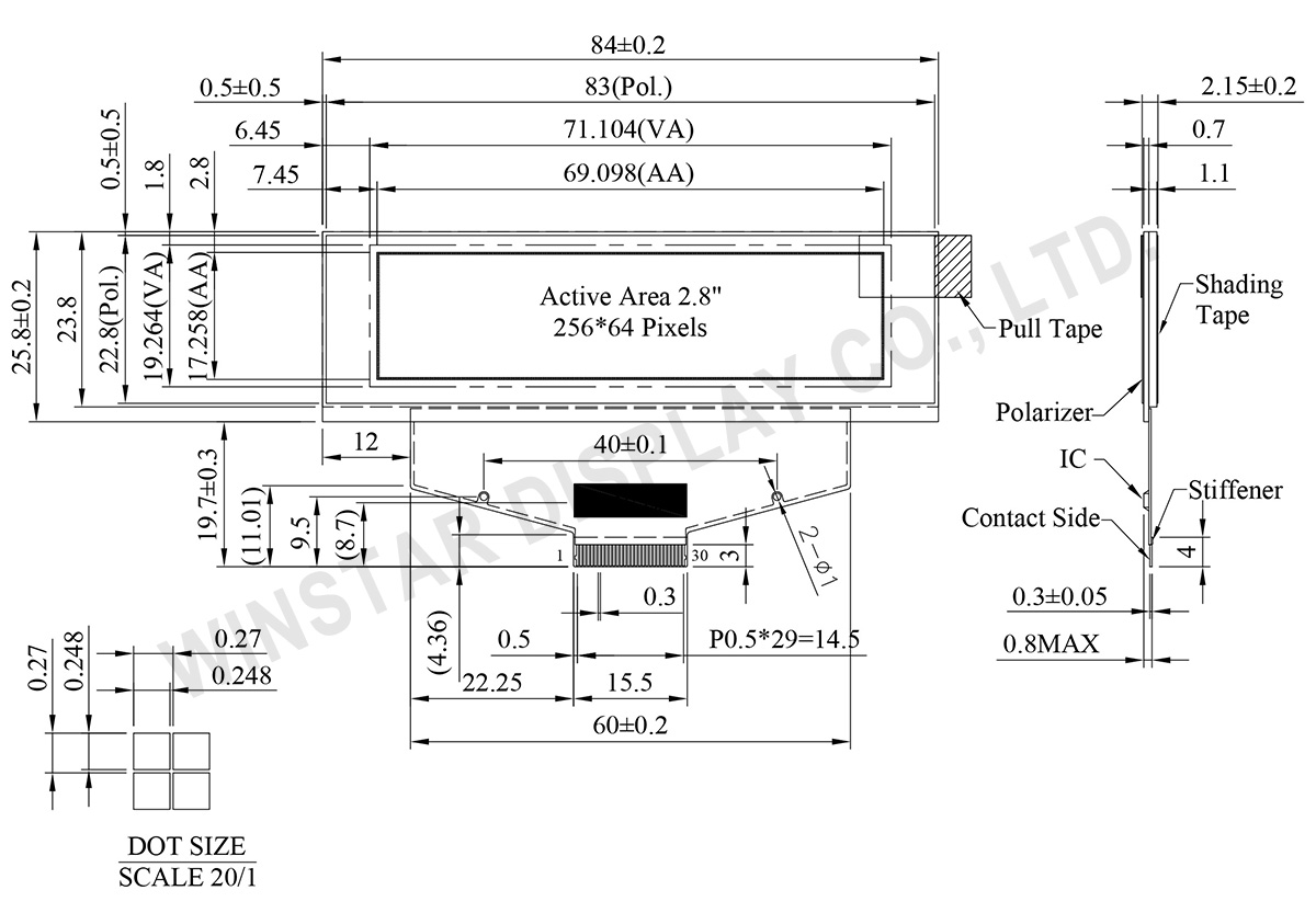
WEX025664Aは、解像度256×64ドットの2.8インチCOFグラフィックOLEDディスプレイモジュールです。SSD1322ドライバICを搭載し、6800、8080、SPIインターフェースに対応しており、各種システムへの柔軟な組み込みが可能です。外形寸法は84.0 × 25.8 × 2.15 mm、表示エリアは69.098 × 17.258 mmです。
本モジュールは、産業機器、POS端末、IoT機器、携帯型測定機器、車載機器、医療機器など幅広い用途に適しています。また、従来のSTNディスプレイからOLEDへの置き換えにも対応可能です。
| 項目 | 仕様 | 単位 |
|---|---|---|
| モジュールサイズ | 256 x 64 Dots | - |
| 表示エリア | 84.0×25.8×2.15 | mm |
| アクティブエリア | 69.098×17.258 | mm |
| ドットサイズ | 0.248×0.248 | mm |
| ドットピッチ | 0.27×0.27 | mm |
| 表示モード | パッシブマトリクス | |
| 表示カラー | モノクロ | |
| 駆動方法 | 1/64 Duty | |
| IC | SSD1322 (COF) | |
| インターフェイス | 6800, 8080, SPI | |
| サイズ | 2.8 インチ | |
| パラメーター | 記号 | 最小値 | 最大値 | 単位 |
|---|---|---|---|---|
| ロジック電源電圧 | VDD | -0.5 | 2.75 | V |
| 低電圧電源 | VCI | -0.3 | 4.0 | V |
| 入力/出力ピンの電源電圧 | VDDIO | -0.5 | VCI | V |
| 表示用電源電圧 | VCC | -0.5 | 20.0 | V |
| 操作温度 | TOP | -40 | +80 | °C |
| 保存温度 | TSTG | -40 | +85 | °C |
| 項目 | 記号 | 条件 | 最小値 | 典型値 | 最大値 | 単位 |
|---|---|---|---|---|---|---|
| ロジック電源電圧 | VCI | Note | 2.8 | 3.0 | 3.3 | V |
| 表示用電源電圧 | VCC | - | 14 | 14.5 | 15 | V |
| 高レベル入力 | VIH | - | 0.8×VDDIO | - | VDDIO | V |
| 低レベル入力 | VIL | - | 0 | - | 0.2×VDDIO | V |
| 高レベル出力 | VOH | - | 0.9×VDDIO | - | VDDIO | V |
| 低レベル出力 | VOL | - | 0 | - | 0.1×VDDIO | V |
| 50% チェックボード動作電流 | VCC =14.5V | 25 | 30 | 32 | mA | |
| Pin Number | 記号 | I/O | 説明 | ||||||||||||||||
|---|---|---|---|---|---|---|---|---|---|---|---|---|---|---|---|---|---|---|---|
| Power Supply | |||||||||||||||||||
| 26 | VCI | P | Power Supply for Operation This is a voltage supply pin. It must be connected to external source & always be equal to or higher than VDD & VDDIO. |
||||||||||||||||
| 25 | VDD | P | Power Supply for Core Logic Circuit This is a voltage supply pin. It can be supplied externally (within the range of 2.4~2.6V) or regulated internally from VCI. A capacitor should be connected between this pin & VSS under all circumstances. |
||||||||||||||||
| 24 | VDDIO | P | Power Supply for I/O Pin This pin is a power supply pin of I/O buffer. It should be connected to VDD or external source. All I/O signal should have VIH reference to VDDIO. When I/O signal pins (BS0~BS1, D0~D7, control signals…) pull high, they should be connected to VDDIO. |
||||||||||||||||
| 2 | VSS | P | Ground of Logic Circuit This is a ground pin. It also acts as a reference for the logic pins. It must be connected to external ground. |
||||||||||||||||
| 3,29 | VCC | P | Power Supply for OLED Panel These are the most positive voltage supply pin of the chip. They must be connected to external source. |
||||||||||||||||
| 5,28 | VLSS | P | Ground of Analog Circuit These are the analog ground pins. They should be connected to VSS externally. |
||||||||||||||||
| Driver | |||||||||||||||||||
| 22 | IREF | I | Current Reference for Brightness Adjustment This pin is segment current reference pin. A resistor should be connected between this pin and VSS. Set the current lower than 10uA. |
||||||||||||||||
| 4 | VCOMH | P | Voltage Output High Level for COM Signal This pin is the input pin for the voltage output high level for COM signals. A tantalum capacitor should be connected between this pin and VSS. |
||||||||||||||||
| 27 | VSL | P | Voltage Output Low Level for SEG Signal This is segment voltage reference pin. When external VSL is not used, this pin should be left open. When external VSL is used, this pin should connect with resistor and diode to ground. |
||||||||||||||||
| Testing Pads | |||||||||||||||||||
| 21 | FR | O | This pin is No Connection pins. Nothing should be connected to this pin. This pin should be left open individually. | ||||||||||||||||
| 16 | BS0 | I | Communicating Protocol Select These pins are MCU interface selection input. See the following table:
|
||||||||||||||||
| 17 | BS1 | ||||||||||||||||||
| 20 | RES# | I | Power Reset for Controller and Driver This pin is reset signal input. When the pin is low, initialization of the chip is executed. |
||||||||||||||||
| 19 | CS# | I | Chip Select This pin is the chip select input. The chip is enabled for MCU communication only when CS# is pulled low. |
||||||||||||||||
| 18 | D/C# | I | Data/Command Control This pin is Data/Command control pin. When the pin is pulled high, the input at D7~D0 is treated as display data. When the pin is pulled low, the input at D7~D0 will be transferred to the command register. For detail relationship to MCU interface signals, please refer to the Timing Characteristics Diagrams. |
||||||||||||||||
| 14 | E/RD# | I | Read/Write Enable or Read This pin is MCU interface input. When interfacing to a 68XX-series microprocessor, this pin will be used as the Enable (E) signal. Read/write operation is initiated when this pin is pulled high and the CS# is pulled low. When connecting to an 80XX-microprocessor, this pin receives the Read (RD#) signal. Data read operation is initiated when this pin is pulled low and CS# is pulled low. When serial mode is selected, this pin must be connected to VSS. |
||||||||||||||||
| 15 | R/W# | I | Read/Write Select or Write This pin is MCU interface input. When interfacing to a 68XX-series microprocessor, this pin will be used as Read/Write (R/W#) selection input. Pull this pin to “High” for read mode and pull it to “Low” for write mode. When 80XX interface mode is selected, this pin will be the Write (WR#) input. Data write operation is initiated when this pin is pulled low and the CS# is pulled low. When serial mode is selected, this pin must be connected to VSS. |
||||||||||||||||
| 6~13 | D7~D0 | I/O | Host Data Input/Output Bus These pins are 8-bit bi-directional data bus to be connected to the microprocessor’s data bus. When serial mode is selected, D1 will be the serial data input SDIN and D0 will be the serial clock input SCLK. Unused pins must be connected to VSS except for D2 in serial mode. |
||||||||||||||||
| Reserve | |||||||||||||||||||
| 23 | N.C. | - | Reserved Pin The N.C. pin between function pins are reserved for compatible and flexible design. |
||||||||||||||||
| 1,30 | N.C. (GND) | - | Reserved Pin (Supporting Pin) The supporting pins can reduce the influences from stresses on the function pins. These pins must be connected to external ground. |
||||||||||||||||

「すべてのクッキーを許可」をクリックすると、サイトのナビゲーションを向上させ、サイト使用状況を分析し、マーケティングおよびパフォーマンスの取り組みを支援するために、クッキーをデバイスに保存することに同意したことになります。この件に関する詳細情報は、ポリシーをご覧ください。プライバシーポリシー