私たちはあなたのプライバシーを大切にします
「すべてのクッキーを許可」をクリックすると、サイトのナビゲーションを向上させ、サイト使用状況を分析し、マーケティングおよびパフォーマンスの取り組みを支援するために、クッキーをデバイスに保存することに同意したことになります。この件に関する詳細情報は、ポリシーをご覧ください。プライバシーポリシー


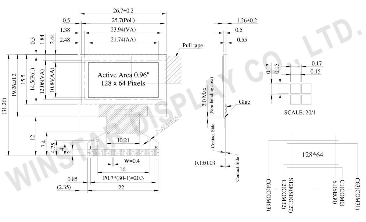
WEO012864ACは、128x64 解像度のコンパクトな0.96インチ I2C OLEDディスプレイで、SSD1315 コントローラICにより駆動されます。この0.96インチ OLED I2Cディスプレイは、I2C、SPI、6800、および8080の複数のインターフェースオプションをサポートし、さまざまなアプリケーションへの柔軟な統合を提供します。
この0.96インチ I2C OLEDディスプレイは、ウェアラブルデバイス、医療機器、産業用制御システムに最適で、スペースと電力効率が重要な用途に適しています。低消費電力で高いパフォーマンスを提供し、1/64のデューティサイクルで駆動され、-40°Cから+80°Cまでの広い動作温度範囲に対応しています。
| 項目 | 仕様 | 単位 |
|---|---|---|
| ドットマトリックス | 128 x 64 | - |
| モジュールサイズ | 26.70 × 19.26 ×1.26 | mm |
| 有効表示エリア | 21.74 × 10.86 | mm |
| ドットサイズ | 0.15 × 0.15 | mm |
| ドットピッチ | 0.17 × 0.17 | mm |
| 表示モード | パッシブマトリクス | |
| 発光色 | モノクロ | |
| 駆動方法 | 1/64 Duty | |
| コントローラー IC | SSD1315 | |
| インターフェイス | 6800, 8080, SPI, I2C | |
| サイズ | 0.96 インチ | |
| パラメーター | 記号 | 最小値 | 最大値 | 単位 |
|---|---|---|---|---|
| ロジック電源電圧 | VDD | 0 | 4.0 | V |
| Power supply for charge pump circuit | VBAT | 0 | 6.0 | V |
| Display電源電圧 | VCC | 0 | 15.0 | V |
| 操作温度 | TOP | -40 | +80 | °C |
| 保存温度 | TSTG | -40 | +85 | °C |
| 項目 | 符號 | 條件 | 最小值 | 典型值 | 最大值 | 單位 |
|---|---|---|---|---|---|---|
| ロジック電源電圧 | VDD | - | 1.65 | 3.0 | 3.3 | V |
| Charge Pump Regulator Supply Voltage | VBAT | - | 2.4 | 3.5 | 5.0 | V |
| Supply Voltage for Display | VCC | - | 6.0 | 12.0 | 12.5 | V |
| Charge Pump Output Voltage for Display (Generated by Internal DC/DC) | Charge Pump VPP |
- | 7.0 | 7.5 | - | V |
| 高レベル入力 | VIH | - | 0.8xVDD | - | VDD | V |
| 低レベル入力 | VIL | - | 0 | - | 0.2xVDD | V |
| 高レベル出力 | VOH | - | 0.9xVDD | - | VDD | V |
| 低レベル出力 | VOL | - | 0 | - | 0.1xVDD | V |
| Operating Current for VCC (50% display ON) (VCC Supplied Externally) | ICC | VCC=12V | - | 10 | 20 | mA |
| 50% checkerboard operating Current (VCC Generated by Internal DC/DC) | IBAT | - | - | 15 | 30 | mA |
| No. | 記号 | 説明 | ||||||||||||||||||||||||
|---|---|---|---|---|---|---|---|---|---|---|---|---|---|---|---|---|---|---|---|---|---|---|---|---|---|---|
| 1 | N.C. (GND) | The supporting pins can reduce the influences from stresses on the function pins. These pins must be connected to external ground. | ||||||||||||||||||||||||
| 2 | C2N | C1P/C1N – Pin for charge pump capacitor; Connect to each other with a capacitor. C2P/C2N – Pin for charge pump capacitor; Connect to each other with a capacitor. |
||||||||||||||||||||||||
| 3 | C2P | |||||||||||||||||||||||||
| 4 | C1P | |||||||||||||||||||||||||
| 5 | C1N | |||||||||||||||||||||||||
| 6 | VBAT | This is the power supply pin for the internal buffer of the DC/DC voltage converter. It must be connected to external source when the converter is used. It should be float when the converter is not used. | ||||||||||||||||||||||||
| 7 | NC | NC | ||||||||||||||||||||||||
| 8 | VSS | Ground pin. It must be connected to external ground. | ||||||||||||||||||||||||
| 9 | VDD | Power supply pin for core logic operation. | ||||||||||||||||||||||||
| 10 | BS0 | These pins are MCU interface selection input. See the following table:
|
||||||||||||||||||||||||
| 11 | BS1 | |||||||||||||||||||||||||
| 12 | BS2 | |||||||||||||||||||||||||
| 13 | CS# | This pin is the chip select input connecting to the MCU. The chip is enabled for MCU communication only when CS# is pulled LOW (active LOW). |
||||||||||||||||||||||||
| 14 | RES# | This pin is reset signal input. When the pin is low, initialization of the chip is executed. Keep this pin HIGH (i.e. connect to VDD) during normal operation. | ||||||||||||||||||||||||
| 15 | D/C# | This is Data/Command control pin. When it is pulled HIGH (i.e. connect to VDD), the data at D[7:0] is treated as data. When it is pulled LOW, the data at D[7:0] will be transferred to the command register. In I2C mode, this pin acts as SA0 for slave address selection. When 3-wire serial interface is selected, this pin must be connected to VSS. For detail relationship to MCU interface signals, please refer to the Timing Characteristics Diagrams of IC SPEC. |
||||||||||||||||||||||||
| 16 | R/W# | This is read / write control input pin connecting to the MCU interface. When interfacing to a 6800-series microprocessor, this pin will be used as Read/Write (R/W#) selection input. Read mode will be carried out when this pin is pulled HIGH (i.e. connect to VDD) and write mode when LOW. When 8080 interface mode is selected, this pin will be the Write (WR#) input. Data write operation is initiated when this pin is pulled LOW and the chip is selected. When serial or I2C interface is selected, this pin must be connected to VSS. |
||||||||||||||||||||||||
| 17 | E/RD# | When interfacing to a 6800-series microprocessor, this pin will be used as the Enable (E) signal. Read/write operation is initiated when this pin is pulled HIGH (i.e. connect to VDD) and the chip is selected. When connecting to an 8080-series microprocessor, this pin receives the Read (RD#) signal. Read operation is initiated when this pin is pulled LOW and the chip is selected. When serial or I2C interface is selected, this pin must be connected to VSS. |
||||||||||||||||||||||||
| 18~25 | D0~D7 | These are 8-bit bi-directional data bus to be connected to the microprocessor’s data bus. When serial interface mode is selected, D0 will be the serial clock input: SCLK; D1 will be the serial data input: SDIN. When I2C mode is selected, D2, D1 should be tied together and serve as SDAout, SDAin in application and D0 is the serial clock input, SCL. |
||||||||||||||||||||||||
| 26 | IREF | When external IREF is used, a resistor should be connected between this pin and VSS to maintain the IREF current at a maximum of 30uA. | ||||||||||||||||||||||||
| 27 | VCOMH | The pin for COM signal deselected voltage level. A capacitor should be connected between this pin and VSS. | ||||||||||||||||||||||||
| 28 | VCC | Power supply for panel driving voltage. This is also the most positive power voltage supply pin. When charge pump is enabled, a capacitor should be connected between this pin and VSS. |
||||||||||||||||||||||||
| 29 | VLSS | This is an analog ground pin. It should be connected to VSS externally. | ||||||||||||||||||||||||
| 30 | NC (GND) |
The supporting pins can reduce the influences from stresses on the function pins. These pins must be connected to external ground. |

「すべてのクッキーを許可」をクリックすると、サイトのナビゲーションを向上させ、サイト使用状況を分析し、マーケティングおよびパフォーマンスの取り組みを支援するために、クッキーをデバイスに保存することに同意したことになります。この件に関する詳細情報は、ポリシーをご覧ください。プライバシーポリシー