

私たちはあなたのプライバシーを大切にします
「すべてのクッキーを許可」をクリックすると、サイトのナビゲーションを向上させ、サイト使用状況を分析し、マーケティングおよびパフォーマンスの取り組みを支援するために、クッキーをデバイスに保存することに同意したことになります。この件に関する詳細情報は、ポリシーをご覧ください。プライバシーポリシー


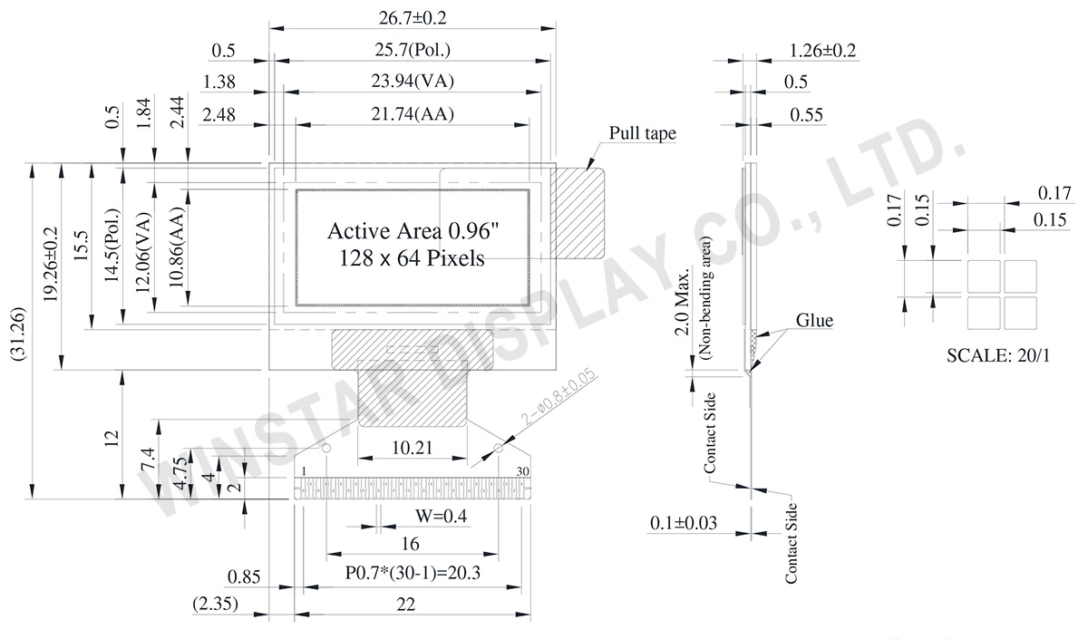
WEO012864ADは、128x64ピクセルの解像度でクリアな表示を提供する0.96インチCOG構造のOLED 128x64 I2Cグラフィックディスプレイです。この0.96インチOLEDスクリーンは、ST7315 ICによって駆動され、I2C、6800または8080パラレル、3/4ラインSPIインターフェースを介して通信できます。表示は、典型的な12Vの供給電圧、1/64駆動デューティ、3.0Vの論理供給電圧(典型)で動作します。50%のチェッカーボード表示(白色)の場合、消費電流は6mA @ 3.0VCCです。WEO012864ADはWEO012864DモデルのIC代替ソリューションで、電気的特性とPFCピン定義が同一であり、互換性のために初期コードの調整のみが必要です。WINSTARの0.96インチOLEDディスプレイモジュールは、SH1106 ICを搭載したWEO012864C、SSD1315 ICを搭載したWEO012864AC、そしてこのST7315 ICを搭載したWEO012864ADなど、さまざまなオプションがあり、お客様のニーズに合わせた柔軟な選択肢を提供します。
この128x64 OLED I2Cモジュールは、スマートホームデバイス、金融POSシステム、クラウド/IoTアプリケーション、インテリジェント技術デバイス、エネルギーシステム、通信システム、医療機器など、さまざまな用途に最適です。動作温度範囲は-40℃から+80℃、保存温度範囲は-40℃から+85℃まで広く、さまざまな環境で使用可能です。
| 項目 | 仕様 | 単位 |
|---|---|---|
| ドットマトリックス | 128 x 64 Dots | - |
| モジュールサイズ | 26.70 × 19.26 ×1.26 | mm |
| 有効表示エリア | 21.74 × 10.86 | mm |
| ドットサイズ | 0.15 × 0.15 | mm |
| ドットピッチ | 0.17 × 0.17 | mm |
| 表示モード | パッシブマトリクス | |
| 発光色 | モノクロ | |
| 駆動方法 | 1/64 Duty | |
| コントローラー IC | ST7315 | |
| インターフェイス | 6800, 8080, SPI, I2C | |
| サイズ | 0.96 インチ | |
| パラメーター | 記号 | 最小値 | 最大値 | 単位 |
|---|---|---|---|---|
| ロジック電源電圧 | VDD | -0.3 | 5.5 | V |
| Display電源電圧 | VOLED | 0 | 18.0 | V |
| 操作温度 | TOP | -40 | +80 | °C |
| 保存温度 | TSTG | -40 | +85 | °C |
| 項目 | 符號 | 條件 | 最小值 | 典型值 | 最大值 | 單位 |
|---|---|---|---|---|---|---|
| ロジック電源電圧 | VDD | - | 2.4 | 3.0 | 5.0 | V |
| Supply Voltage for Display (Supplied Externally) |
VOLED | - | 7.5 | 12.0 | 16.5 | V |
| Charge Pump Regulator Supply Voltage |
VBAT | - | 3.0 | 3.5 | 5.0 | V |
| Charge Pump Output Voltage for Display (Generated by Internal DC/DC) | Charge Pump VOLED |
- | 7.0 | 7.5 | - | V |
| 高レベル入力 | VIH | - | 0.8×VDD | - | - | V |
| 低レベル入力 | VIL | - | - | - | 0.2×VDD | V |
| 高レベル出力 | VOH | - | 0.9×VDD | - | - | V |
| 低レベル出力 | VOL | - | - | - | 0.1×VDD | V |
| Display 50% Pixel on Operating Current for VOLED (VOLED Supplied Externally) |
IOLED | VOLED=12V | - | 6 | 12 | mA |
| Display 50% Pixel on (VOLED Generated by Internal DC/DC) |
IBAT | VBAT=3.5V | - | 15 | 30 | mA |
| No. | 記号 | 説明 | ||||||||||||||||||||||||
|---|---|---|---|---|---|---|---|---|---|---|---|---|---|---|---|---|---|---|---|---|---|---|---|---|---|---|
| 1 | N.C. (GND) | The supporting pins can reduce the influences from stresses on the function pins. These pins must be connected to external ground. | ||||||||||||||||||||||||
| 2 | C2N | DC/DC voltage converter. Connect a capacitor between CA1P and CA1N. Connect a capacitor between CA2P and CA2N. |
||||||||||||||||||||||||
| 3 | C2P | |||||||||||||||||||||||||
| 4 | C1P | |||||||||||||||||||||||||
| 5 | C1N | |||||||||||||||||||||||||
| 6 | VBAT | Analog power for internal booster. If VDD=VABT | ||||||||||||||||||||||||
| 7 | NC | NC | ||||||||||||||||||||||||
| 8 | DGND | Digital ground. Connect to GND | ||||||||||||||||||||||||
| 9 | VDD | Power supply pin for core logic operation. | ||||||||||||||||||||||||
| 10 | IF0 | These pins select interface operation mode.
|
||||||||||||||||||||||||
| 11 | IF1 | |||||||||||||||||||||||||
| 12 | IF2 | |||||||||||||||||||||||||
| 13 | CSB | Chip select input pin. CSB=“L”: This chip is selected and the MPU interface is active. CSB=“H”: This chip is not selected and the MPU interface is disabled (D[7:0] are high impedance). |
||||||||||||||||||||||||
| 14 | RSTB | This pin is reset signal input. When the pin is low, initialization of the chip is executed. Keep this pin HIGH (i.e. connect to VDD) during normal operation. | ||||||||||||||||||||||||
| 15 | A0 | It determines whether the access is related to data or command. A0 = "H": Indicates that D[7:0] are display data; A0 = "L": Indicates that D[7:0] are control data. This pin is I2C slave address bit (SA0), when I2C interface is selected. |
||||||||||||||||||||||||
| 16 | RWR | Read / Write execution control pin. (This pin is only used in parallel interface)
This pin is not used in serial interfaces and should be connected to DGND. |
||||||||||||||||||||||||
| 17 | ERD | Read / Write execution control pin. (This pin is only used in parallel interface)
This pin is not used in serial interfaces and should be connected to DGND. |
||||||||||||||||||||||||
| 18~25 | D0~D7 | When using 8-bit parallel interface: 8080 or 6800 mode 8 bit bi-directional data bus. Connect to the data bus of 8-bit microprocessor. When CSB is “H”, D[7:0] are high impedance. When using serial interface : 3-line SPI or 4-line SPI mode D[2:1] : serial input/output data (SDA). D[0] : serial input clock (SCL). D1 to D2 must be connected together (SDA) D[7:3] : fix to “L” by DGND. When using serial interface : I2C interface D[2] : SDA_OUT, serial data and acknowledge output for the I2C interface. D[1] : SDA_IN, serial input data D[0] : SCL, serial input clock . D1 to D2 must be connected together (SDA) D[7:3] : fix to “L” by DGND. |
||||||||||||||||||||||||
| 26 | IREF | Internal IREF is used, please leave this pin open. | ||||||||||||||||||||||||
| 27 | VCOMH | VCOMH is the driving voltage for common and segment circuits. | ||||||||||||||||||||||||
| 28 | VOLED | VOLED is the diving voltage for segment circuit. | ||||||||||||||||||||||||
| 29 | PGND | Analog ground. Connect to GND | ||||||||||||||||||||||||
| 30 | NC (GND) |
The supporting pins can reduce the influences from stresses on the function pins. These pins must be connected to external ground. |

「すべてのクッキーを許可」をクリックすると、サイトのナビゲーションを向上させ、サイト使用状況を分析し、マーケティングおよびパフォーマンスの取り組みを支援するために、クッキーをデバイスに保存することに同意したことになります。この件に関する詳細情報は、ポリシーをご覧ください。プライバシーポリシー