
我們重視您的隱私
通過點擊「允許所有 Cookie」,代表您同意在您的設備上存儲 Cookie 以增強網站瀏覽體驗、分析網站使用情況並協助我們的行銷和網站效能優化工作。您可以在我們的隱私權政策中找到有關於此的更多資訊。


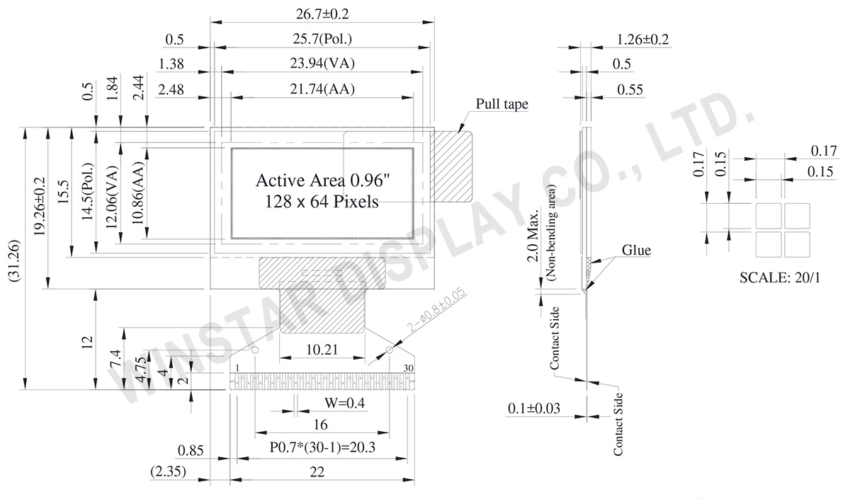
WEO012864AD為COG結構0.96吋繪圖型OLED顯示器模組,顯示畫面由128x64 dots組成。此OLED模組內建ST7315 IC,有8-bit 6800 / 8080、3線/4線 SPI 和 I2C等多種介面可選擇。WEO012864AD顯示電壓 typical value 12V, 邏輯電壓 typical value 3V,驅動方式1/64 duty, 50%顯示畫面耗電流為6 [email protected] (白色)。WEO012864AD型號是WEO012864D型號的 IC 替代解決方案; 電氣特性和PFC引腳定義相同,客戶只需調整初始代碼。 Winstar 0.96吋 OLED 有許多替代選擇,例如WEO012864C 型號內建SH1106 IC,WEO012864AC型號內建SSD1315 IC ,以及WEO012864AD型號內建 ST7315 IC 。
WEO012864AD型號適用於智能家居應用、金融POS、Cloud/IoT systems、智能技術設備、能源系統、通信系統、醫療儀器等。模組操作溫度範圍-40~+80°C;儲存溫度範圍-40~+85°C。
| 項目 | 規格 | 單位 |
|---|---|---|
| 點陣(解析度) | 128 x 64 Dots | - |
| 模組尺寸 | 26.70 x 19.26 x 1.26 | mm |
| 有效區域 | 21.74 x 10.86 | mm |
| 點大小 | 0.15 x 0.15 | mm |
| 點間距 | 0.17 x 0.17 | mm |
| 顯示模式 | 被動矩陣 | |
| 發光顏色 | 單色 | |
| 驅動方式 | 1/64 Duty | |
| 控制器IC | ST7315 | |
| 介面 | 6800, 8080, SPI, I2C | |
| 尺寸 | 0.96 吋 | |
| 參數 | 符號 | 最小值 | 最大值 | 單位 |
|---|---|---|---|---|
| 邏輯電源電壓 | VDD | -0.3 | 5.5 | V |
| 顯示電源電壓 | VOLED | 0 | 18.0 | V |
| 工作溫度 | TOP | -40 | +80 | °C |
| 儲存溫度 | TSTG | -40 | +85 | °C |
| 項目 | 符號 | 條件 | 最小值 | 典型值 | 最大值 | 單位 |
|---|---|---|---|---|---|---|
| 邏輯電源電壓 | VDD | - | 2.4 | 3.0 | 5.0 | V |
| 顯示電源電壓 | VOLED | - | 7.5 | 12.0 | 16.5 | V |
| 電荷幫浦穩壓器電源電壓 | VBAT | - | 3.0 | 3.5 | 5.0 | V |
| 顯示器的電荷幫浦輸出電壓 (Generated by Internal DC/DC) |
Charge Pump VOLED |
- | 7.0 | 7.5 | - | V |
| 輸入高準位 | VIH | - | 0.8×VDD | - | - | V |
| 輸入低準位 | VIL | - | - | - | 0.2×VDD | V |
| 輸出高準位 | VOH | - | 0.9×VDD | - | - | V |
| 輸出低準位 | VOL | - | - | - | 0.1×VDD | V |
| Display 50% Pixel on Operating Current for VOLED (VOLED Supplied Externally) |
IOLED | VOLED=12V | - | 6 | 12 | mA |
| Display 50% Pixel on (VOLED Generated by Internal DC/DC) |
IBAT | VBAT=3.5V | - | 15 | 30 | mA |
| No. | 符號 | 功能說明 | ||||||||||||||||||||||||
|---|---|---|---|---|---|---|---|---|---|---|---|---|---|---|---|---|---|---|---|---|---|---|---|---|---|---|
| 1 | N.C. (GND) | The supporting pins can reduce the influences from stresses on the function pins. These pins must be connected to external ground. | ||||||||||||||||||||||||
| 2 | C2N | DC/DC voltage converter. Connect a capacitor between CA1P and CA1N. Connect a capacitor between CA2P and CA2N. |
||||||||||||||||||||||||
| 3 | C2P | |||||||||||||||||||||||||
| 4 | C1P | |||||||||||||||||||||||||
| 5 | C1N | |||||||||||||||||||||||||
| 6 | VBAT | Analog power for internal booster. If VDD=VABT | ||||||||||||||||||||||||
| 7 | NC | NC | ||||||||||||||||||||||||
| 8 | DGND | Digital ground. Connect to GND | ||||||||||||||||||||||||
| 9 | VDD | Power supply pin for core logic operation. | ||||||||||||||||||||||||
| 10 | IF0 | These pins select interface operation mode.
|
||||||||||||||||||||||||
| 11 | IF1 | |||||||||||||||||||||||||
| 12 | IF2 | |||||||||||||||||||||||||
| 13 | CSB | Chip select input pin. CSB=“L”: This chip is selected and the MPU interface is active. CSB=“H”: This chip is not selected and the MPU interface is disabled (D[7:0] are high impedance). |
||||||||||||||||||||||||
| 14 | RSTB | This pin is reset signal input. When the pin is low, initialization of the chip is executed. Keep this pin HIGH (i.e. connect to VDD) during normal operation. | ||||||||||||||||||||||||
| 15 | A0 | It determines whether the access is related to data or command. A0 = "H": Indicates that D[7:0] are display data; A0 = "L": Indicates that D[7:0] are control data. This pin is I2C slave address bit (SA0), when I2C interface is selected. |
||||||||||||||||||||||||
| 16 | RWR | Read / Write execution control pin. (This pin is only used in parallel interface)
This pin is not used in serial interfaces and should be connected to DGND. |
||||||||||||||||||||||||
| 17 | ERD | Read / Write execution control pin. (This pin is only used in parallel interface)
This pin is not used in serial interfaces and should be connected to DGND. |
||||||||||||||||||||||||
| 18~25 | D0~D7 | When using 8-bit parallel interface: 8080 or 6800 mode 8 bit bi-directional data bus. Connect to the data bus of 8-bit microprocessor. When CSB is “H”, D[7:0] are high impedance. When using serial interface : 3-line SPI or 4-line SPI mode D[2:1] : serial input/output data (SDA). D[0] : serial input clock (SCL). D1 to D2 must be connected together (SDA) D[7:3] : fix to “L” by DGND. When using serial interface : I2C interface D[2] : SDA_OUT, serial data and acknowledge output for the I2C interface. D[1] : SDA_IN, serial input data D[0] : SCL, serial input clock . D1 to D2 must be connected together (SDA) D[7:3] : fix to “L” by DGND. |
||||||||||||||||||||||||
| 26 | IREF | Internal IREF is used, please leave this pin open. | ||||||||||||||||||||||||
| 27 | VCOMH | VCOMH is the driving voltage for common and segment circuits. | ||||||||||||||||||||||||
| 28 | VOLED | VOLED is the diving voltage for segment circuit. | ||||||||||||||||||||||||
| 29 | PGND | Analog ground. Connect to GND | ||||||||||||||||||||||||
| 30 | NC (GND) |
The supporting pins can reduce the influences from stresses on the function pins. These pins must be connected to external ground. |

通過點擊「允許所有 Cookie」,代表您同意在您的設備上存儲 Cookie 以增強網站瀏覽體驗、分析網站使用情況並協助我們的行銷和網站效能優化工作。您可以在我們的隱私權政策中找到有關於此的更多資訊。