El modelo WEO012864AD es una pantalla gráfica OLED de 0,96 pulgadas con estructura COG, que ofrece una visualización clara con una resolución de 128x64 píxeles. Esta pantalla OLED 0,96" está alimentada por el IC ST7315 y soporta comunicación a través de I2C, paralelo 6800 o 8080 y interfaces SPI de 3/4 líneas. La pantalla funciona con un voltaje de alimentación típico de 12V, con un ciclo de conducción de 1/64 y un voltaje de alimentación lógica de 3,0V (valor típico). Con una visualización en tablero de ajedrez al 50% (color blanco), el consumo de corriente es de 6mA @ 3,0VCC. El modelo WEO012864AD sirve como una alternativa IC al modelo WEO012864D, con características eléctricas y definiciones de pines PFC idénticas, requiriendo solo pequeños ajustes en el código inicial para garantizar la compatibilidad. Los módulos de pantalla OLED 0,96" de WINSTAR están disponibles en varias opciones, como el WEO012864C con IC SH1106, el WEO012864AC con IC SSD1315 y este WEO012864AD con IC ST7315, brindando a los clientes flexibilidad para elegir la solución adecuada para sus aplicaciones.
Este módulo 128x64 OLED I2C es ideal para su uso en dispositivos de automatización del hogar, sistemas POS financieros, aplicaciones Cloud/IoT, dispositivos tecnológicos inteligentes, sistemas de energía, sistemas de comunicación, instrumentos médicos y más. Opera en un amplio rango de temperatura de -40℃ a +80℃ y tiene un rango de temperatura de almacenamiento de -40℃ a +85℃, lo que lo hace adecuado para una variedad de entornos.
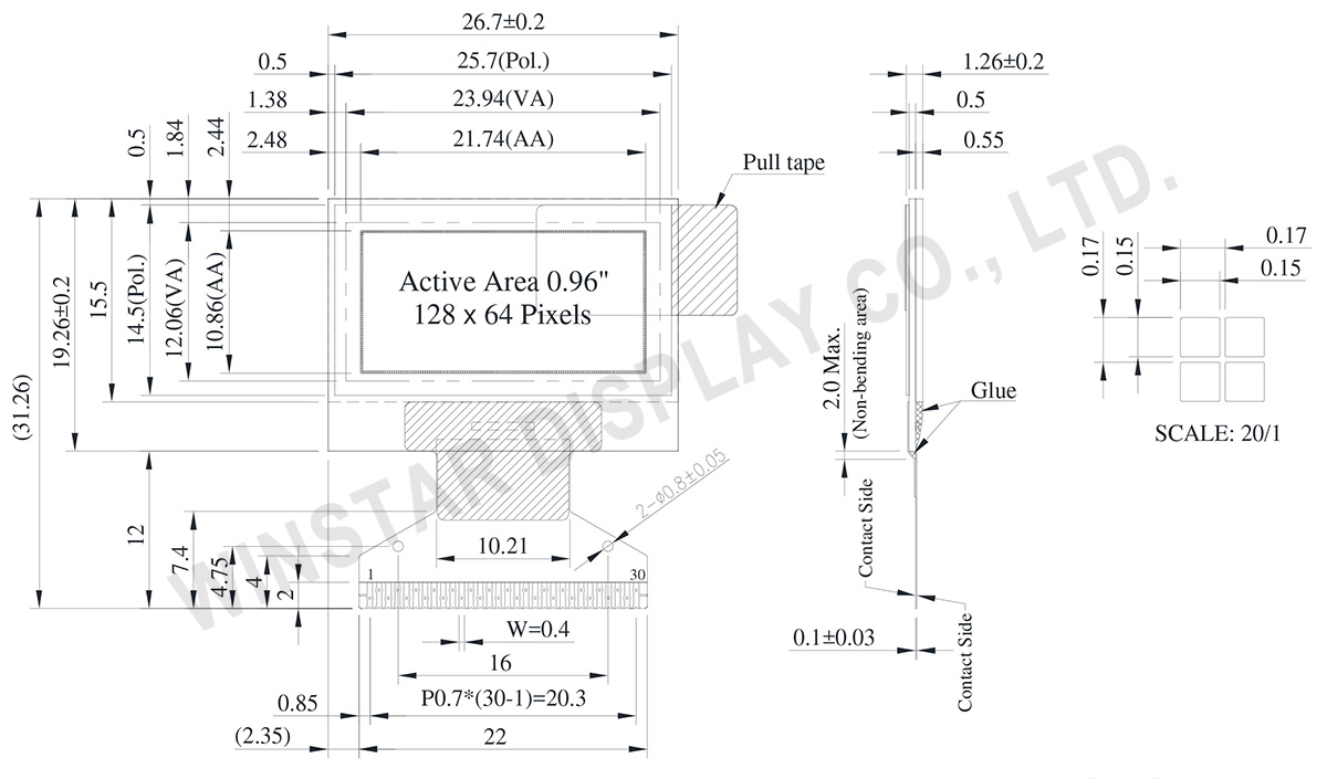
DIBUJO
Data source ref:WEO012864ADWPP3N00000
ESPECIFICACIONES
Especificaciones generales
Elemento
Dimensión
Unidad
Matriz de puntos
128 x 64 Dots
-
Dimensión del módulo
26.70 × 19.26 ×1.26
mm
zona activa
21.74 × 10.86
mm
Tamaño del punto
0.15 × 0.15
mm
Distancia entre puntos
0.17 × 0.17
mm
Modo de visualización
Matriz pasiva
Color de la pantalla
Monocromos
Drive Duty
1/64 Duty
IC de Controlador
ST7315
Interfaz
6800, 8080, SPI, I2C
Tamaño
0.96 pulgada
Valores nominales máximos absolutos
Parameter
Símbolo
Valor mín.
Valor máx.
Unidad
Supply Voltage for Logic
VDD
-0.3
5.5
V
Supply Voltage for Display
VOLED
0
18.0
V
Temperatura de funcionamiento
TOP
-40
+80
°C
Temperatura de almacenamiento
TSTG
-40
+85
°C
Características electrónicas
DC Características electrónicas
Elemento
Símbolo
Condición
Valor mín.
Valor típico
Valor máx.
Unidad
Supply Voltage for Logic
VDD
-
2.4
3.0
5.0
V
Supply Voltage for Display
(Supplied Externally)
VOLED
-
7.5
12.0
16.5
V
Charge Pump Regulator
Supply Voltage
VBAT
-
3.0
3.5
5.0
V
Charge Pump Output Voltage for Display (Generated by Internal DC/DC)
Charge Pump
VOLED
-
7.0
7.5
-
V
Input High Volt.
VIH
-
0.8×VDD
-
-
V
Input Low Volt.
VIL
-
-
-
0.2×VDD
V
Output High Volt.
VOH
-
0.9×VDD
-
-
V
Output Low Volt.
VOL
-
-
-
0.1×VDD
V
Display 50% Pixel on
Operating Current for VOLED
(VOLED Supplied Externally)
IOLED
VOLED=12V
-
6
12
mA
Display 50% Pixel on
(VOLED Generated by Internal DC/DC)
IBAT
VBAT=3.5V
-
15
30
mA
Función interfaz Pin
No.
Símbolo
Función
1
N.C. (GND)
The supporting pins can reduce the influences from stresses on the function pins. These pins must be connected to external ground.
2
C2N
DC/DC voltage converter.
Connect a capacitor between CA1P and CA1N.
Connect a capacitor between CA2P and CA2N.
3
C2P
4
C1P
5
C1N
6
VBAT
Analog power for internal booster. If VDD=VABT
7
NC
NC
8
DGND
Digital ground. Connect to GND
9
VDD
Power supply pin for core logic operation.
10
IF0
These pins select interface operation mode.
IF2
IF1
IF0
MPU interface type
L
L
L
4-line serial interface
L
L
H
3-line serial interface
L
H
L
I2C serial interface
H
H
L
8-bit 8080 parallel interface
H
L
L
8-bit 6800 parallel interface
11
IF1
12
IF2
13
CSB
Chip select input pin.
CSB=“L”: This chip is selected and the MPU interface is active.
CSB=“H”: This chip is not selected and the MPU interface is disabled (D[7:0] are high impedance).
14
RSTB
This pin is reset signal input. When the pin is low, initialization of the chip is executed. Keep this pin HIGH (i.e. connect to VDD) during normal operation.
15
A0
It determines whether the access is related to data or command.
A0 = "H": Indicates that D[7:0] are display data;
A0 = "L": Indicates that D[7:0] are control data.
This pin is I2C slave address bit (SA0), when I2C interface is selected.
16
RWR
Read / Write execution control pin. (This pin is only used in parallel interface)
Write enable input pin.
The data are latched at the rising edge of th /WR signal.
This pin is not used in serial interfaces and should be connected to DGND.
17
ERD
Read / Write execution control pin. (This pin is only used in parallel interface)
MPU Type
ERD
Description
6800-series
ERD
Read / Write control input pin.
R/W = "H": When E is "H", data bus is in output status.
R/W = "L": The data are latched at the falling edge of the E signal.
8080-series
/RD
Read enable input pin.
When /RD is "L", data bus is in output status.
This pin is not used in serial interfaces and should be connected to DGND.
18~25
D0~D7
When using 8-bit parallel interface: 8080 or 6800 mode 8 bit bi-directional data bus. Connect to the data bus of 8-bit microprocessor. When CSB is “H”, D[7:0] are high impedance. When using serial interface : 3-line SPI or 4-line SPI mode
D[2:1] : serial input/output data (SDA).
D[0] : serial input clock (SCL).
D1 to D2 must be connected together (SDA)
D[7:3] : fix to “L” by DGND. When using serial interface : I2C interface
D[2] : SDA_OUT, serial data and acknowledge output for the I2C interface.
D[1] : SDA_IN, serial input data
D[0] : SCL, serial input clock .
D1 to D2 must be connected together (SDA)
D[7:3] : fix to “L” by DGND.
26
IREF
Internal IREF is used, please leave this pin open.
27
VCOMH
VCOMH is the driving voltage for common and segment circuits.
28
VOLED
VOLED is the diving voltage for segment circuit.
29
PGND
Analog ground. Connect to GND
30
NC
(GND)
The supporting pins can reduce the influences from stresses on the function pins. These pins must be connected to external ground.
Al hacer clic en "Permitir todas las cookies", aceptas el almacenamiento de cookies en tu dispositivo para mejorar la navegación en el sitio, analizar el uso del sitio y ayudar en nuestros esfuerzos de marketing y rendimiento. Puedes encontrar más información sobre este tema en nuestra política. Política de privacidad


 - WEO012864U")
