Il modello WEO012864AD è un display grafico OLED con struttura COG da 0,96 pollici, con una risoluzione di 128x64 pixel che garantisce immagini chiare. Questo schermo OLED 0,96" è alimentato dal chip ST7315 e supporta la comunicazione tramite interfacce I2C, parallelo 6800 o 8080 e SPI a 3/4 linee. Il display funziona con una tensione di alimentazione tipica di 12V, un duty cycle di 1/64 e una tensione di alimentazione logica di 3,0V (valore tipico). Con una visualizzazione a scacchiera al 50% (colore bianco), il consumo di corrente è di 6mA @ 3,0VCC. Il modello WEO012864AD è una soluzione alternativa IC per il modello WEO012864D, con caratteristiche elettriche e definizioni dei pin PFC identiche, richiedendo solo una leggera modifica del codice iniziale per la compatibilità. I moduli display OLED 0,96" di WINSTAR sono disponibili in varie opzioni, come WEO012864C con IC SH1106, WEO012864AC con IC SSD1315 e questo WEO012864AD con IC ST7315, offrendo ai clienti una scelta flessibile per le loro applicazioni.
Questo modulo 128x64 OLED I2C è ideale per dispositivi smart home, sistemi POS finanziari, applicazioni Cloud/IoT, dispositivi tecnologici intelligenti, sistemi energetici, sistemi di comunicazione, dispositivi medici e altro. Funziona in un intervallo di temperatura compreso tra -40℃ e +80℃, con una temperatura di conservazione che va da -40℃ a +85℃, rendendolo adatto a una vasta gamma di ambienti.
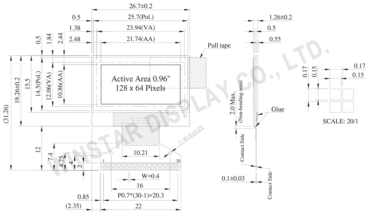
DISEGNO
Data source ref:WEO012864ADWPP3N00000
SPECIFICHE TECNICHE
Specifiche generali
Articolo
Dimensioni
Unità
A matrice di punti
128 x 64 Dots
-
Dimensione del modulo
26.70 × 19.26 ×1.26
mm
Area attiva
21.74 × 10.86
mm
Dimensioni del Dot
0.15 × 0.15
mm
Passo del Dot
0.17 × 0.17
mm
Modalità display
Matrice passiva
Colore display
monocromatici
Drive Duty
1/64 Duty
Controllo IC
ST7315
Interfaccia
6800, 8080, SPI, I2C
Dimensione (Diagonale)
0.96 pollici
Valori massimi assoluti
Parameter
Simbolo
Valore Min
Valore massimo
Unità
Supply Voltage for Logic
VDD
-0.3
5.5
V
Supply Voltage for Display
VOLED
0
18.0
V
Temperatura di lavoro
TOP
-40
+80
°C
Temperatura di stock
TSTG
-40
+85
°C
Caratteristiche elettriche
DC Caratteristiche elettriche
Articolo
Simbolo
Condizione
Valore Min
Valore tipico
Valore massimo
Unità
Supply Voltage for Logic
VDD
-
2.4
3.0
5.0
V
Supply Voltage for Display
(Supplied Externally)
VOLED
-
7.5
12.0
16.5
V
Charge Pump Regulator
Supply Voltage
VBAT
-
3.0
3.5
5.0
V
Charge Pump Output Voltage for Display (Generated by Internal DC/DC)
Charge Pump
VOLED
-
7.0
7.5
-
V
Input High Volt.
VIH
-
0.8×VDD
-
-
V
Input Low Volt.
VIL
-
-
-
0.2×VDD
V
Output High Volt.
VOH
-
0.9×VDD
-
-
V
Output Low Volt.
VOL
-
-
-
0.1×VDD
V
Display 50% Pixel on
Operating Current for VOLED
(VOLED Supplied Externally)
IOLED
VOLED=12V
-
6
12
mA
Display 50% Pixel on
(VOLED Generated by Internal DC/DC)
IBAT
VBAT=3.5V
-
15
30
mA
Funzione dei Pin di Interfaccia
No.
Simbolo
Funzione
1
N.C. (GND)
The supporting pins can reduce the influences from stresses on the function pins. These pins must be connected to external ground.
2
C2N
DC/DC voltage converter.
Connect a capacitor between CA1P and CA1N.
Connect a capacitor between CA2P and CA2N.
3
C2P
4
C1P
5
C1N
6
VBAT
Analog power for internal booster. If VDD=VABT
7
NC
NC
8
DGND
Digital ground. Connect to GND
9
VDD
Power supply pin for core logic operation.
10
IF0
These pins select interface operation mode.
IF2
IF1
IF0
MPU interface type
L
L
L
4-line serial interface
L
L
H
3-line serial interface
L
H
L
I2C serial interface
H
H
L
8-bit 8080 parallel interface
H
L
L
8-bit 6800 parallel interface
11
IF1
12
IF2
13
CSB
Chip select input pin.
CSB=“L”: This chip is selected and the MPU interface is active.
CSB=“H”: This chip is not selected and the MPU interface is disabled (D[7:0] are high impedance).
14
RSTB
This pin is reset signal input. When the pin is low, initialization of the chip is executed. Keep this pin HIGH (i.e. connect to VDD) during normal operation.
15
A0
It determines whether the access is related to data or command.
A0 = "H": Indicates that D[7:0] are display data;
A0 = "L": Indicates that D[7:0] are control data.
This pin is I2C slave address bit (SA0), when I2C interface is selected.
16
RWR
Read / Write execution control pin. (This pin is only used in parallel interface)
Write enable input pin.
The data are latched at the rising edge of th /WR signal.
This pin is not used in serial interfaces and should be connected to DGND.
17
ERD
Read / Write execution control pin. (This pin is only used in parallel interface)
MPU Type
ERD
Description
6800-series
ERD
Read / Write control input pin.
R/W = "H": When E is "H", data bus is in output status.
R/W = "L": The data are latched at the falling edge of the E signal.
8080-series
/RD
Read enable input pin.
When /RD is "L", data bus is in output status.
This pin is not used in serial interfaces and should be connected to DGND.
18~25
D0~D7
When using 8-bit parallel interface: 8080 or 6800 mode 8 bit bi-directional data bus. Connect to the data bus of 8-bit microprocessor. When CSB is “H”, D[7:0] are high impedance. When using serial interface : 3-line SPI or 4-line SPI mode
D[2:1] : serial input/output data (SDA).
D[0] : serial input clock (SCL).
D1 to D2 must be connected together (SDA)
D[7:3] : fix to “L” by DGND. When using serial interface : I2C interface
D[2] : SDA_OUT, serial data and acknowledge output for the I2C interface.
D[1] : SDA_IN, serial input data
D[0] : SCL, serial input clock .
D1 to D2 must be connected together (SDA)
D[7:3] : fix to “L” by DGND.
26
IREF
Internal IREF is used, please leave this pin open.
27
VCOMH
VCOMH is the driving voltage for common and segment circuits.
28
VOLED
VOLED is the diving voltage for segment circuit.
29
PGND
Analog ground. Connect to GND
30
NC
(GND)
The supporting pins can reduce the influences from stresses on the function pins. These pins must be connected to external ground.
Facendo clic su "Consenti tutti i cookie", accetti la memorizzazione dei cookie sul tuo dispositivo per migliorare la navigazione del sito, analizzare l'utilizzo del sito e assistere nei nostri sforzi di marketing e prestazioni. Puoi trovare ulteriori informazioni su questo argomento nella nostra politica. Informativa sulla privacy


 - WEO012864C")
 - WEO012864Y")
