우리는 귀하의 프라이버시를 소중히 여깁니다
"모든 쿠키 허용"을 클릭하면 사이트 탐색을 개선하고, 사이트 사용을 분석하며, 마케팅 및 성능 노력에 도움을 주기 위해 쿠키를 귀하의 장치에 저장하는 데 동의한 것으로 간주됩니다. 이 주제에 대한 추가 정보는 당사의 정책에서 확인할 수 있습니다. 개인정보 보호정책


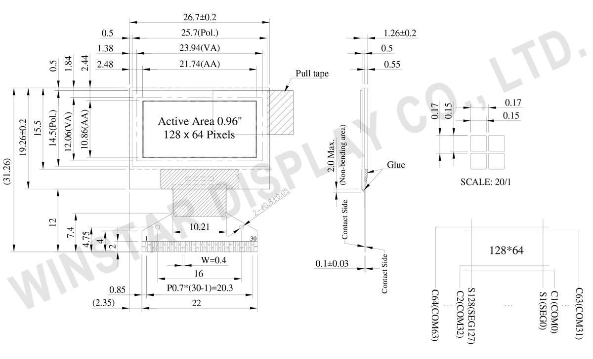
WEO012864AC는 128x64 해상도를 갖춘 컴팩트한 0.96인치 I2C OLED 디스플레이로, SSD1315 컨트롤러 IC에 의해 구동됩니다. 이 0.96인치 OLED I2C 디스플레이는 I2C, SPI, 6800, 8080 등 다양한 인터페이스 옵션을 지원하여 여러 애플리케이션에 유연하게 적용할 수 있습니다.
이 0.96인치 I2C OLED 디스플레이는 웨어러블 디바이스, 의료 기기, 산업용 제어 시스템에 적합하며, 공간과 전력 효율성이 중요한 경우에 이상적입니다. 이 디스플레이는 낮은 전력 소비와 높은 성능을 제공하며, 1/64 듀티 사이클로 구동되어 -40°C에서 +80°C까지의 넓은 동작 온도 범위를 지원합니다.
| 항목 | 치수 | 단위 |
|---|---|---|
| 도트 매트릭스 | 128 x 64 | - |
| 모듈 치수 | 26.70 × 19.26 ×1.26 | mm |
| 활성 영역 | 21.74 × 10.86 | mm |
| 도트 크기 | 0.15 × 0.15 | mm |
| 도트 피치 | 0.17 × 0.17 | mm |
| 디스플레이 모드 | 패시브 매트릭스 | |
| 디스플레이 색상 | Monochrome | |
| Drive Duty | 1/64 Duty | |
| 제어 IC | SSD1315 | |
| 인터페이스 | 6800, 8080, SPI, I2C | |
| 크기 | 0.96 인치 | |
| Parameter | 기호 | 최소값 | 최대값 | 단위 |
|---|---|---|---|---|
| Supply Voltage for Logic | VDD | 0 | 4.0 | V |
| Power supply for charge pump circuit | VBAT | 0 | 6.0 | V |
| Supply Voltage for Display | VCC | 0 | 15.0 | V |
| 작동 온도 | TOP | -40 | +80 | °C |
| 보관 온도 | TSTG | -40 | +85 | °C |
| 항목 | 기호 | 조건 | 최소값 | 대표값 | 최대값 | 단위 |
|---|---|---|---|---|---|---|
| Supply Voltage for Logic | VDD | - | 1.65 | 3.0 | 3.3 | V |
| Charge Pump Regulator Supply Voltage | VBAT | - | 2.4 | 3.5 | 5.0 | V |
| Supply Voltage for Display | VCC | - | 6.0 | 12.0 | 12.5 | V |
| Charge Pump Output Voltage for Display (Generated by Internal DC/DC) | Charge Pump VPP |
- | 7.0 | 7.5 | - | V |
| Input High Volt. | VIH | - | 0.8xVDD | - | VDD | V |
| Input Low Volt. | VIL | - | 0 | - | 0.2xVDD | V |
| Output High Volt. | VOH | - | 0.9xVDD | - | VDD | V |
| Output Low Volt. | VOL | - | 0 | - | 0.1xVDD | V |
| Operating Current for VCC (50% display ON) (VCC Supplied Externally) | ICC | VCC=12V | - | 10 | 20 | mA |
| 50% checkerboard operating Current (VCC Generated by Internal DC/DC) | IBAT | - | - | 15 | 30 | mA |
| No. | 기호 | 기능 | ||||||||||||||||||||||||
|---|---|---|---|---|---|---|---|---|---|---|---|---|---|---|---|---|---|---|---|---|---|---|---|---|---|---|
| 1 | N.C. (GND) | The supporting pins can reduce the influences from stresses on the function pins. These pins must be connected to external ground. | ||||||||||||||||||||||||
| 2 | C2N | C1P/C1N – Pin for charge pump capacitor; Connect to each other with a capacitor. C2P/C2N – Pin for charge pump capacitor; Connect to each other with a capacitor. |
||||||||||||||||||||||||
| 3 | C2P | |||||||||||||||||||||||||
| 4 | C1P | |||||||||||||||||||||||||
| 5 | C1N | |||||||||||||||||||||||||
| 6 | VBAT | This is the power supply pin for the internal buffer of the DC/DC voltage converter. It must be connected to external source when the converter is used. It should be float when the converter is not used. | ||||||||||||||||||||||||
| 7 | NC | NC | ||||||||||||||||||||||||
| 8 | VSS | Ground pin. It must be connected to external ground. | ||||||||||||||||||||||||
| 9 | VDD | Power supply pin for core logic operation. | ||||||||||||||||||||||||
| 10 | BS0 | These pins are MCU interface selection input. See the following table:
|
||||||||||||||||||||||||
| 11 | BS1 | |||||||||||||||||||||||||
| 12 | BS2 | |||||||||||||||||||||||||
| 13 | CS# | This pin is the chip select input connecting to the MCU. The chip is enabled for MCU communication only when CS# is pulled LOW (active LOW). |
||||||||||||||||||||||||
| 14 | RES# | This pin is reset signal input. When the pin is low, initialization of the chip is executed. Keep this pin HIGH (i.e. connect to VDD) during normal operation. | ||||||||||||||||||||||||
| 15 | D/C# | This is Data/Command control pin. When it is pulled HIGH (i.e. connect to VDD), the data at D[7:0] is treated as data. When it is pulled LOW, the data at D[7:0] will be transferred to the command register. In I2C mode, this pin acts as SA0 for slave address selection. When 3-wire serial interface is selected, this pin must be connected to VSS. For detail relationship to MCU interface signals, please refer to the Timing Characteristics Diagrams of IC SPEC. |
||||||||||||||||||||||||
| 16 | R/W# | This is read / write control input pin connecting to the MCU interface. When interfacing to a 6800-series microprocessor, this pin will be used as Read/Write (R/W#) selection input. Read mode will be carried out when this pin is pulled HIGH (i.e. connect to VDD) and write mode when LOW. When 8080 interface mode is selected, this pin will be the Write (WR#) input. Data write operation is initiated when this pin is pulled LOW and the chip is selected. When serial or I2C interface is selected, this pin must be connected to VSS. |
||||||||||||||||||||||||
| 17 | E/RD# | When interfacing to a 6800-series microprocessor, this pin will be used as the Enable (E) signal. Read/write operation is initiated when this pin is pulled HIGH (i.e. connect to VDD) and the chip is selected. When connecting to an 8080-series microprocessor, this pin receives the Read (RD#) signal. Read operation is initiated when this pin is pulled LOW and the chip is selected. When serial or I2C interface is selected, this pin must be connected to VSS. |
||||||||||||||||||||||||
| 18~25 | D0~D7 | These are 8-bit bi-directional data bus to be connected to the microprocessor’s data bus. When serial interface mode is selected, D0 will be the serial clock input: SCLK; D1 will be the serial data input: SDIN. When I2C mode is selected, D2, D1 should be tied together and serve as SDAout, SDAin in application and D0 is the serial clock input, SCL. |
||||||||||||||||||||||||
| 26 | IREF | When external IREF is used, a resistor should be connected between this pin and VSS to maintain the IREF current at a maximum of 30uA. | ||||||||||||||||||||||||
| 27 | VCOMH | The pin for COM signal deselected voltage level. A capacitor should be connected between this pin and VSS. | ||||||||||||||||||||||||
| 28 | VCC | Power supply for panel driving voltage. This is also the most positive power voltage supply pin. When charge pump is enabled, a capacitor should be connected between this pin and VSS. |
||||||||||||||||||||||||
| 29 | VLSS | This is an analog ground pin. It should be connected to VSS externally. | ||||||||||||||||||||||||
| 30 | NC (GND) |
The supporting pins can reduce the influences from stresses on the function pins. These pins must be connected to external ground. |

"모든 쿠키 허용"을 클릭하면 사이트 탐색을 개선하고, 사이트 사용을 분석하며, 마케팅 및 성능 노력에 도움을 주기 위해 쿠키를 귀하의 장치에 저장하는 데 동의한 것으로 간주됩니다. 이 주제에 대한 추가 정보는 당사의 정책에서 확인할 수 있습니다. 개인정보 보호정책