我們重視您的隱私
通過點擊「允許所有 Cookie」,代表您同意在您的設備上存儲 Cookie 以增強網站瀏覽體驗、分析網站使用情況並協助我們的行銷和網站效能優化工作。您可以在我們的隱私權政策中找到有關於此的更多資訊。


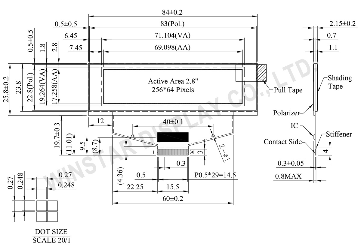
WEX025664A 為一款 2.8 吋 COF 繪圖型 OLED 顯示模組,解析度為 256×64 dots。此模組搭載 SSD1322 驅動 IC,並支援 6800、8080 與 SPI 介面,可靈活整合至各類系統設計中。模組外形尺寸為 84.0 × 25.8 × 2.15 mm,顯示區域為 69.098 × 17.258 mm。
此模組適用於工業設備、POS 系統、IoT 裝置、手持式儀器、車載設備及醫療設備等應用,同時亦可作為傳統 STN 顯示器升級至 OLED 技術的解決方案。
| 項目 | 尺寸 | 單位 |
|---|---|---|
| 點陣 | 256 x 64 Dots | - |
| 模組尺寸 | 84.0×25.8×2.15 | mm |
| 有效區域 | 69.098×17.258 | mm |
| 像素大小 | 0.248×0.248 | mm |
| 像素間距 | 0.27×0.27 | mm |
| 顯示模組 | 被動矩陣 | |
| 顯示顏色 | 單色 | |
| 驅動方式 | 1/64 Duty | |
| IC | SSD1322 (COF) | |
| 介面 | 6800, 8080, SPI | |
| 尺寸 | 2.8 吋 | |
| 參數 | 符號 | 最小值 | 最大值 | 單位 |
|---|---|---|---|---|
| 邏輯電源電壓 | VDD | -0.5 | 2.75 | V |
| 低壓電源 | VCI | -0.3 | 4.0 | V |
| 輸入/輸出Pin供電電壓 | VDDIO | -0.5 | VCI | V |
| 顯示電源電壓 | VCC | -0.5 | 20.0 | V |
| 工作溫度 | TOP | -40 | +80 | °C |
| 儲存溫度 | TSTG | -40 | +85 | °C |
| 項目 | 符號 | 條件 | 最小值 | 典型值 | 最大值 | 單位 |
|---|---|---|---|---|---|---|
| 邏輯電源電壓 | VCI | Note | 2.8 | 3.0 | 3.3 | V |
| 顯示電源電壓 | VCC | - | 14 | 14.5 | 15 | V |
| 輸入高準位 | VIH | - | 0.8×VDDIO | - | VDDIO | V |
| 輸入低準位 | VIL | - | 0 | - | 0.2×VDDIO | V |
| 輸出高準位 | VOH | - | 0.9×VDDIO | - | VDDIO | V |
| 輸出低準位 | VOL | - | 0 | - | 0.1×VDDIO | V |
| 50% 設備運行電流 | VCC =14.5V | 25 | 30 | 32 | mA | |
| Pin Number | 符號 | I/O | 功能說明 | ||||||||||||||||
|---|---|---|---|---|---|---|---|---|---|---|---|---|---|---|---|---|---|---|---|
| Power Supply | |||||||||||||||||||
| 26 | VCI | P | Power Supply for Operation This is a voltage supply pin. It must be connected to external source & always be equal to or higher than VDD & VDDIO. |
||||||||||||||||
| 25 | VDD | P | Power Supply for Core Logic Circuit This is a voltage supply pin. It can be supplied externally (within the range of 2.4~2.6V) or regulated internally from VCI. A capacitor should be connected between this pin & VSS under all circumstances. |
||||||||||||||||
| 24 | VDDIO | P | Power Supply for I/O Pin This pin is a power supply pin of I/O buffer. It should be connected to VDD or external source. All I/O signal should have VIH reference to VDDIO. When I/O signal pins (BS0~BS1, D0~D7, control signals…) pull high, they should be connected to VDDIO. |
||||||||||||||||
| 2 | VSS | P | Ground of Logic Circuit This is a ground pin. It also acts as a reference for the logic pins. It must be connected to external ground. |
||||||||||||||||
| 3,29 | VCC | P | Power Supply for OLED Panel These are the most positive voltage supply pin of the chip. They must be connected to external source. |
||||||||||||||||
| 5,28 | VLSS | P | Ground of Analog Circuit These are the analog ground pins. They should be connected to VSS externally. |
||||||||||||||||
| Driver | |||||||||||||||||||
| 22 | IREF | I | Current Reference for Brightness Adjustment This pin is segment current reference pin. A resistor should be connected between this pin and VSS. Set the current lower than 10uA. |
||||||||||||||||
| 4 | VCOMH | P | Voltage Output High Level for COM Signal This pin is the input pin for the voltage output high level for COM signals. A tantalum capacitor should be connected between this pin and VSS. |
||||||||||||||||
| 27 | VSL | P | Voltage Output Low Level for SEG Signal This is segment voltage reference pin. When external VSL is not used, this pin should be left open. When external VSL is used, this pin should connect with resistor and diode to ground. |
||||||||||||||||
| Testing Pads | |||||||||||||||||||
| 21 | FR | O | This pin is No Connection pins. Nothing should be connected to this pin. This pin should be left open individually. | ||||||||||||||||
| 16 | BS0 | I | Communicating Protocol Select These pins are MCU interface selection input. See the following table:
|
||||||||||||||||
| 17 | BS1 | ||||||||||||||||||
| 20 | RES# | I | Power Reset for Controller and Driver This pin is reset signal input. When the pin is low, initialization of the chip is executed. |
||||||||||||||||
| 19 | CS# | I | Chip Select This pin is the chip select input. The chip is enabled for MCU communication only when CS# is pulled low. |
||||||||||||||||
| 18 | D/C# | I | Data/Command Control This pin is Data/Command control pin. When the pin is pulled high, the input at D7~D0 is treated as display data. When the pin is pulled low, the input at D7~D0 will be transferred to the command register. For detail relationship to MCU interface signals, please refer to the Timing Characteristics Diagrams. |
||||||||||||||||
| 14 | E/RD# | I | Read/Write Enable or Read This pin is MCU interface input. When interfacing to a 68XX-series microprocessor, this pin will be used as the Enable (E) signal. Read/write operation is initiated when this pin is pulled high and the CS# is pulled low. When connecting to an 80XX-microprocessor, this pin receives the Read (RD#) signal. Data read operation is initiated when this pin is pulled low and CS# is pulled low. When serial mode is selected, this pin must be connected to VSS. |
||||||||||||||||
| 15 | R/W# | I | Read/Write Select or Write This pin is MCU interface input. When interfacing to a 68XX-series microprocessor, this pin will be used as Read/Write (R/W#) selection input. Pull this pin to “High” for read mode and pull it to “Low” for write mode. When 80XX interface mode is selected, this pin will be the Write (WR#) input. Data write operation is initiated when this pin is pulled low and the CS# is pulled low. When serial mode is selected, this pin must be connected to VSS. |
||||||||||||||||
| 6~13 | D7~D0 | I/O | Host Data Input/Output Bus These pins are 8-bit bi-directional data bus to be connected to the microprocessor’s data bus. When serial mode is selected, D1 will be the serial data input SDIN and D0 will be the serial clock input SCLK. Unused pins must be connected to VSS except for D2 in serial mode. |
||||||||||||||||
| Reserve | |||||||||||||||||||
| 23 | N.C. | - | Reserved Pin The N.C. pin between function pins are reserved for compatible and flexible design. |
||||||||||||||||
| 1,30 | N.C. (GND) | - | Reserved Pin (Supporting Pin) The supporting pins can reduce the influences from stresses on the function pins. These pins must be connected to external ground. |
||||||||||||||||

通過點擊「允許所有 Cookie」,代表您同意在您的設備上存儲 Cookie 以增強網站瀏覽體驗、分析網站使用情況並協助我們的行銷和網站效能優化工作。您可以在我們的隱私權政策中找到有關於此的更多資訊。