우리는 귀하의 프라이버시를 소중히 여깁니다
"모든 쿠키 허용"을 클릭하면 사이트 탐색을 개선하고, 사이트 사용을 분석하며, 마케팅 및 성능 노력에 도움을 주기 위해 쿠키를 귀하의 장치에 저장하는 데 동의한 것으로 간주됩니다. 이 주제에 대한 추가 정보는 당사의 정책에서 확인할 수 있습니다. 개인정보 보호정책


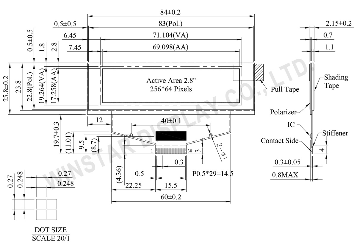
WEX025664A는 256×64 해상도를 지원하는 2.8인치 COF 그래픽 OLED 디스플레이 모듈입니다. SSD1322 드라이버 IC를 탑재하고 있으며, 6800, 8080, SPI 인터페이스를 지원하여 다양한 시스템 설계에 유연하게 적용할 수 있습니다. 모듈 외형 크기는 84.0 x 25.8 x 2.15 mm, 표시 영역은 69.098 x 17.258 mm입니다.
본 모듈은 산업용 장비, POS 시스템, IoT 기기, 휴대형 계측 장비, 자동차 전장, 의료 기기 등 다양한 분야에 적합합니다. 또한 기존 STN 디스플레이를 OLED로 대체하는 업그레이드 용도로도 활용할 수 있습니다.
| 항목 | 치수 | 단위 |
|---|---|---|
| 도트 매트릭스 | 256 x 64 Dots | - |
| 모듈 치수 | 84.0×25.8×2.15 | mm |
| 활성 영역 | 69.098×17.258 | mm |
| 픽셀 크기 | 0.248×0.248 | mm |
| 픽셀 피치 | 0.27×0.27 | mm |
| 디스플레이 모드 | 패시브 매트릭스 | |
| 디스플레이 색상 | 단색 | |
| 구동 듀티비 | 1/64 Duty | |
| IC | SSD1322 (COF) | |
| 인터페이스 | 6800, 8080, SPI | |
| 크기(대각선) | 2.8 inch | |
| 항목 | 기호 | 최소값 | 최대값 | 단위 |
|---|---|---|---|---|
| 로직 전원 전압 | VDD | -0.5 | 2.75 | V |
| 저전압 전원 | VCI | -0.3 | 4.0 | V |
| I/O 전원 전압 | VDDIO | -0.5 | VCI | V |
| 디스플레이 구동 전압 | VCC | -0.5 | 20.0 | V |
| 동작 온도 | TOP | -40 | +80 | °C |
| 보관 온도 | TSTG | -40 | +85 | °C |
| 항목 | 기호 | 조건 | 최소값 | 전형값 | 최대값 | 단위 |
|---|---|---|---|---|---|---|
| 로직 전원 전압 | VCI | Note | 2.8 | 3.0 | 3.3 | V |
| 디스플레이 전원 전압 | VCC | - | 14 | 14.5 | 15 | V |
| 입력 High 전압 | VIH | - | 0.8×VDDIO | - | VDDIO | V |
| 입력 Low 전압 | VIL | - | 0 | - | 0.2×VDDIO | V |
| 출력 High 전압 | VOH | - | 0.9×VDDIO | - | VDDIO | V |
| 출력 Low 전압 | VOL | - | 0 | - | 0.1×VDDIO | V |
| 50% 보드 동작 전류 | VCC =14.5V | 25 | 30 | 32 | mA | |
| Pin Number | 기호 | I/O | 기능 | ||||||||||||||||
|---|---|---|---|---|---|---|---|---|---|---|---|---|---|---|---|---|---|---|---|
| Power Supply | |||||||||||||||||||
| 26 | VCI | P | Power Supply for Operation This is a voltage supply pin. It must be connected to external source & always be equal to or higher than VDD & VDDIO. |
||||||||||||||||
| 25 | VDD | P | Power Supply for Core Logic Circuit This is a voltage supply pin. It can be supplied externally (within the range of 2.4~2.6V) or regulated internally from VCI. A capacitor should be connected between this pin & VSS under all circumstances. |
||||||||||||||||
| 24 | VDDIO | P | Power Supply for I/O Pin This pin is a power supply pin of I/O buffer. It should be connected to VDD or external source. All I/O signal should have VIH reference to VDDIO. When I/O signal pins (BS0~BS1, D0~D7, control signals…) pull high, they should be connected to VDDIO. |
||||||||||||||||
| 2 | VSS | P | Ground of Logic Circuit This is a ground pin. It also acts as a reference for the logic pins. It must be connected to external ground. |
||||||||||||||||
| 3,29 | VCC | P | Power Supply for OLED Panel These are the most positive voltage supply pin of the chip. They must be connected to external source. |
||||||||||||||||
| 5,28 | VLSS | P | Ground of Analog Circuit These are the analog ground pins. They should be connected to VSS externally. |
||||||||||||||||
| Driver | |||||||||||||||||||
| 22 | IREF | I | Current Reference for Brightness Adjustment This pin is segment current reference pin. A resistor should be connected between this pin and VSS. Set the current lower than 10uA. |
||||||||||||||||
| 4 | VCOMH | P | Voltage Output High Level for COM Signal This pin is the input pin for the voltage output high level for COM signals. A tantalum capacitor should be connected between this pin and VSS. |
||||||||||||||||
| 27 | VSL | P | Voltage Output Low Level for SEG Signal This is segment voltage reference pin. When external VSL is not used, this pin should be left open. When external VSL is used, this pin should connect with resistor and diode to ground. |
||||||||||||||||
| Testing Pads | |||||||||||||||||||
| 21 | FR | O | This pin is No Connection pins. Nothing should be connected to this pin. This pin should be left open individually. | ||||||||||||||||
| 16 | BS0 | I | Communicating Protocol Select These pins are MCU interface selection input. See the following table:
|
||||||||||||||||
| 17 | BS1 | ||||||||||||||||||
| 20 | RES# | I | Power Reset for Controller and Driver This pin is reset signal input. When the pin is low, initialization of the chip is executed. |
||||||||||||||||
| 19 | CS# | I | Chip Select This pin is the chip select input. The chip is enabled for MCU communication only when CS# is pulled low. |
||||||||||||||||
| 18 | D/C# | I | Data/Command Control This pin is Data/Command control pin. When the pin is pulled high, the input at D7~D0 is treated as display data. When the pin is pulled low, the input at D7~D0 will be transferred to the command register. For detail relationship to MCU interface signals, please refer to the Timing Characteristics Diagrams. |
||||||||||||||||
| 14 | E/RD# | I | Read/Write Enable or Read This pin is MCU interface input. When interfacing to a 68XX-series microprocessor, this pin will be used as the Enable (E) signal. Read/write operation is initiated when this pin is pulled high and the CS# is pulled low. When connecting to an 80XX-microprocessor, this pin receives the Read (RD#) signal. Data read operation is initiated when this pin is pulled low and CS# is pulled low. When serial mode is selected, this pin must be connected to VSS. |
||||||||||||||||
| 15 | R/W# | I | Read/Write Select or Write This pin is MCU interface input. When interfacing to a 68XX-series microprocessor, this pin will be used as Read/Write (R/W#) selection input. Pull this pin to “High” for read mode and pull it to “Low” for write mode. When 80XX interface mode is selected, this pin will be the Write (WR#) input. Data write operation is initiated when this pin is pulled low and the CS# is pulled low. When serial mode is selected, this pin must be connected to VSS. |
||||||||||||||||
| 6~13 | D7~D0 | I/O | Host Data Input/Output Bus These pins are 8-bit bi-directional data bus to be connected to the microprocessor’s data bus. When serial mode is selected, D1 will be the serial data input SDIN and D0 will be the serial clock input SCLK. Unused pins must be connected to VSS except for D2 in serial mode. |
||||||||||||||||
| Reserve | |||||||||||||||||||
| 23 | N.C. | - | Reserved Pin The N.C. pin between function pins are reserved for compatible and flexible design. |
||||||||||||||||
| 1,30 | N.C. (GND) | - | Reserved Pin (Supporting Pin) The supporting pins can reduce the influences from stresses on the function pins. These pins must be connected to external ground. |
||||||||||||||||

"모든 쿠키 허용"을 클릭하면 사이트 탐색을 개선하고, 사이트 사용을 분석하며, 마케팅 및 성능 노력에 도움을 주기 위해 쿠키를 귀하의 장치에 저장하는 데 동의한 것으로 간주됩니다. 이 주제에 대한 추가 정보는 당사의 정책에서 확인할 수 있습니다. 개인정보 보호정책