 I2C 인터페이스 - SSD1315 IC | WEA012864V")
우리는 귀하의 프라이버시를 소중히 여깁니다
"모든 쿠키 허용"을 클릭하면 사이트 탐색을 개선하고, 사이트 사용을 분석하며, 마케팅 및 성능 노력에 도움을 주기 위해 쿠키를 귀하의 장치에 저장하는 데 동의한 것으로 간주됩니다. 이 주제에 대한 추가 정보는 당사의 정책에서 확인할 수 있습니다. 개인정보 보호정책


WEO012864V는 128x64 해상도를 지원하는 0.96인치 COG 그래픽 OLED 디스플레이 모듈로, SSD1315 OLED IC로 구동됩니다. 소비자용 애플리케이션을 위해 설계된 이 SSD1315 OLED 디스플레이는 뛰어난 선명도와 낮은 전력 소비를 제공하여 컴팩트하고 효율적인 시스템에 적합합니다. 이 모듈은 I2C와 SPI (3-wire/4-wire) 통신 인터페이스를 지원하여 다양한 애플리케이션에 쉽게 통합할 수 있습니다.
이 모듈은 3V 논리 전압과 7.5V 디스플레이 전압으로 동작하며, 7.5V VCC에서 6mA의 전류를 소모합니다 (50% 체크보드 디스플레이 기준). 구동 듀티는 1/64이며, 내장된 차지 펌프와 외부 VCC 전원 공급을 모두 지원합니다. 이 SSD1315 OLED 디스플레이는 웨어러블 디바이스, 스마트 홈 애플리케이션 등 다양한 용도에 적합하며, 작동 온도 범위는 -30℃에서 +70℃입니다.
PCB 통합이 필요한 경우, WEA012864V 모델을 선택하실 수 있습니다.
| 항목 | 치수 | 단위 |
|---|---|---|
| 도트 매트릭스 | 128 x 64 Dots | - |
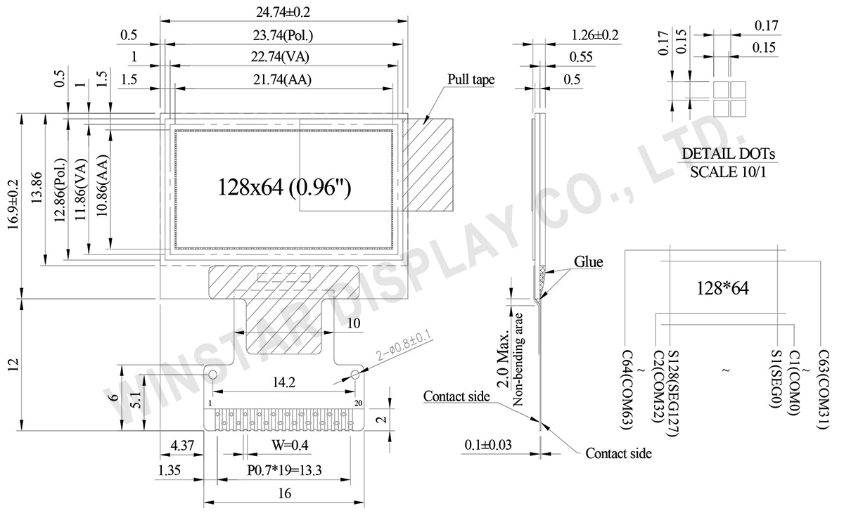
| 모듈 치수 | 24.74 x 16.90 x 1.26 | mm |
| 활성 영역 | 21.74 x 10.86 | mm |
| 도트 크기 | 0.15 x 0.15 | mm |
| 도트 피치 | 0.17 x 0.17 | mm |
| 디스플레이 모드 | 패시브 매트릭스 | |
| 디스플레이 색상 | Monochrome | |
| Drive Duty | 1/64 Duty | |
| IC | SSD1315 | |
| 인터페이스 | 4-line/3-line SPI, I2C | |
| 크기 | 0.96 인치 | |
| Parameter | 기호 | 최소값 | 최대값 | 단위 |
|---|---|---|---|---|
| Supply Voltage for Logic | VDD | -0.3 | 4.0 | V |
| Charge Pump Regulator | VBAT | -0.3 | 6.0 | V |
| Supply Voltage for Display | VCC | 0 | 18.0 | V |
| 작동 온도 | TOP | -30 | +70 | °C |
| 보관 온도 | TSTG | -30 | +70 | °C |
| 항목 | 기호 | 조건 | 최소값 | 대표값 | 최대값 | 단위 |
|---|---|---|---|---|---|---|
| Supply Voltage for Logic | VDD | - | 2.8 | 3.0 | 3.3 | V |
| Supply Voltage for Display | VCC | - | 7.0 | 7.5 | 8.0 | V |
| Input High Volt. | VIH | - | 0.8×VDD | - | VDD | V |
| Input Low Volt. | VIL | - | 0 | - | 0.2×VDD | V |
| Output High Volt. | VOH | - | 0.9×VDD | - | VDD | V |
| Output Low Volt. | VOL | - | 0 | - | 0.1×VDD | V |
| Operating Current for VCC (50% display ON) | ICC | - | - | 6 | 12 | mA |
| No. | 기호 | 기능 | ||||||||
|---|---|---|---|---|---|---|---|---|---|---|
| 1 | C2N | C2P/C2N – Pin for charge pump capacitor; Connect to each other with a capacitor. | ||||||||
| 2 | C2P | |||||||||
| 3 | C1P | C1P/C1N – Pin for charge pump capacitor; Connect to each other with a capacitor. | ||||||||
| 4 | C1N | |||||||||
| 5 | VBAT | Power Supply for DC/DC Converter Circuit This is the power supply pin for the internal buffer of the DC/DC voltage converter. It must be connected to external source when the converter is used. It should be float when the converter is not used. |
||||||||
| 6 | VCC | Power supply for panel driving voltage. This is also the most positive power voltage supply pin. When charge pump is enabled, a capacitor should be connected between this pin and VSS. |
||||||||
| 7 | VSS | Ground of Logic Circuit This is a ground pin. It acts as a reference for the logic pins. It must be connected to external ground. |
||||||||
| 8 | VDD | Power Supply for Logic This is a voltage supply pin. It must be connected to external source. |
||||||||
| 9 | BS0 | Communicating Protocol Select These pins are MCU interface selection input. See the following table:
|
||||||||
| 10 | BS1 | |||||||||
| 11 | CS# | Chip Select This pin is the chip select input. The chip is enabled for MCU communication only when CS# is pulled low. |
||||||||
| 12 | RES# | Power Reset for Controller and Driver This pin is reset signal input. When the pin is low, initialization of the chip is executed. |
||||||||
| 13 | D/C# | In I2C mode, this pin acts as SA0 for slave address selection. When 3-wire serial interface is selected, this pin must be connected to VSS. |
||||||||
| 14~16 | D0~D2 | When serial interface mode is selected, D0 will be the serial clock input: SCLK; D1 will be the serial data input: SDIN. When I2C mode is selected, D2, D1 should be tied together and serve as SDAout, SDAin in application and D0 is the serial clock input, SCL. |
||||||||
| 17 | IREF | Current Reference for Brightness Adjustment This pin is segment current reference pin. A resistor should be connected between this pin and VSS. Set the current lower than 30uA. |
||||||||
| 18 | VCOMH | COM signal deselected voltage level. A capacitor should be connected between this pin and VSS. |
||||||||
| 19 | VCC | Power supply for panel driving voltage. This is also the most positive power voltage supply pin. When charge pump is enabled, a capacitor should be connected between this pin and VSS. |
||||||||
| 20 | VLSS | Ground of Analog Circuit This is an analog ground pin. It should be connected to VSS externally. |

"모든 쿠키 허용"을 클릭하면 사이트 탐색을 개선하고, 사이트 사용을 분석하며, 마케팅 및 성능 노력에 도움을 주기 위해 쿠키를 귀하의 장치에 저장하는 데 동의한 것으로 간주됩니다. 이 주제에 대한 추가 정보는 당사의 정책에서 확인할 수 있습니다. 개인정보 보호정책