 - I2C介面, SSD1315 IC | WEA012864V")
我們重視您的隱私
通過點擊「允許所有 Cookie」,代表您同意在您的設備上存儲 Cookie 以增強網站瀏覽體驗、分析網站使用情況並協助我們的行銷和網站效能優化工作。您可以在我們的隱私權政策中找到有關於此的更多資訊。


WEO012864V是一款0.96吋的COG繪圖型OLED顯示模組,解析度為128x64,由SSD1315 OLED IC提供驅動。此SSD1315 OLED顯示模組專為消費等級應用設計,提供清晰顯示效果及低功耗,適用於小型且高效能的應用。WEO012864V模組支援I2C與3線/4線SPI介面,提供靈活性,輕鬆整合於各種應用。
WEO012864V模組工作時需要3V邏輯電源與7.5V顯示電壓,在50%顯示畫面時,耗電流為6mA(工作電壓:7.5V),驅動週期為1/64。可支援內部升壓及外部供電。這款SSD1315 OLED顯示模組適用於穿戴式設備、智慧家居應用等,工作溫度範圍為-30℃至+70℃。
如果您需要PCB整合,可以選擇型號WEA012864V。
| 項目 | 標準值 | 單位 |
|---|---|---|
| 解析度 | 128 x 64 Dots | - |
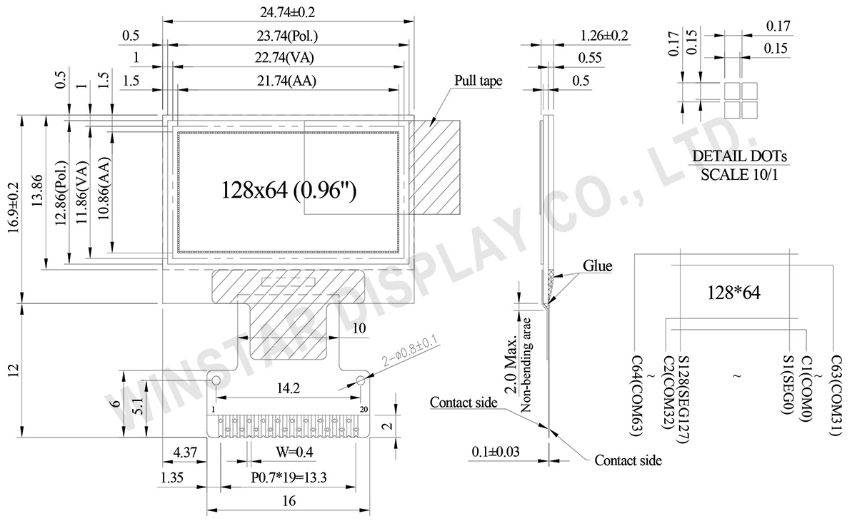
| 模組尺寸 | 24.74 x 16.90 x 1.26 | mm |
| 有效區域 | 21.74 x 10.86 | mm |
| 像素大小 | 0.15 x 0.15 | mm |
| 像素間距 | 0.17 x 0.17 | mm |
| 顯示模式 | 被動矩陣 | |
| 顯示顏色 | 單色 | |
| 驅動方式 | 1/64 Duty | |
| 控制器IC | SSD1315 | |
| 介面 | 4線/3線 SPI, I2C | |
| 尺寸 | 0.96 吋 | |
| 參數 | 符號 | 最小值 | 最大值 | 單位 |
|---|---|---|---|---|
| 邏輯電源電壓 | VDD | -0.3 | 4.0 | V |
| 電荷幫浦穩壓器 | VBAT | -0.3 | 6.0 | V |
| 顯示電源電壓 | VCC | 0 | 18.0 | V |
| 工作溫度 | TOP | -30 | +70 | °C |
| 儲存溫度 | TSTG | -30 | +70 | °C |
| 項目 | 符號 | 條件 | 最小值 | 典型值 | 最大值 | 單位 |
|---|---|---|---|---|---|---|
| 邏輯電源電壓 | VDD | - | 2.8 | 3.0 | 3.3 | V |
| 顯示電源電壓 | VCC | - | 7.0 | 7.5 | 8.0 | V |
| 輸入高準位 | VIH | - | 0.8×VDD | - | VDD | V |
| 輸入低準位 | VIL | - | 0 | - | 0.2×VDD | V |
| 輸出高準位 | VOH | - | 0.9×VDD | - | VDD | V |
| 輸出低準位 | VOL | - | 0 | - | 0.1×VDD | V |
| VCC的工作電流 (50% display ON) | ICC | - | - | 6 | 12 | mA |
| No. | 符號 | 功能說明 | ||||||||
|---|---|---|---|---|---|---|---|---|---|---|
| 1 | C2N | C2P/C2N – Pin for charge pump capacitor; Connect to each other with a capacitor. | ||||||||
| 2 | C2P | |||||||||
| 3 | C1P | C1P/C1N – Pin for charge pump capacitor; Connect to each other with a capacitor. | ||||||||
| 4 | C1N | |||||||||
| 5 | VBAT | Power Supply for DC/DC Converter Circuit This is the power supply pin for the internal buffer of the DC/DC voltage converter. It must be connected to external source when the converter is used. It should be float when the converter is not used. |
||||||||
| 6 | VCC | Power supply for panel driving voltage. This is also the most positive power voltage supply pin. When charge pump is enabled, a capacitor should be connected between this pin and VSS. |
||||||||
| 7 | VSS | Ground of Logic Circuit This is a ground pin. It acts as a reference for the logic pins. It must be connected to external ground. |
||||||||
| 8 | VDD | Power Supply for Logic This is a voltage supply pin. It must be connected to external source. |
||||||||
| 9 | BS0 | Communicating Protocol Select These pins are MCU interface selection input. See the following table:
|
||||||||
| 10 | BS1 | |||||||||
| 11 | CS# | Chip Select This pin is the chip select input. The chip is enabled for MCU communication only when CS# is pulled low. |
||||||||
| 12 | RES# | Power Reset for Controller and Driver This pin is reset signal input. When the pin is low, initialization of the chip is executed. |
||||||||
| 13 | D/C# | In I2C mode, this pin acts as SA0 for slave address selection. When 3-wire serial interface is selected, this pin must be connected to VSS. |
||||||||
| 14~16 | D0~D2 | When serial interface mode is selected, D0 will be the serial clock input: SCLK; D1 will be the serial data input: SDIN. When I2C mode is selected, D2, D1 should be tied together and serve as SDAout, SDAin in application and D0 is the serial clock input, SCL. |
||||||||
| 17 | IREF | Current Reference for Brightness Adjustment This pin is segment current reference pin. A resistor should be connected between this pin and VSS. Set the current lower than 30uA. |
||||||||
| 18 | VCOMH | COM signal deselected voltage level. A capacitor should be connected between this pin and VSS. |
||||||||
| 19 | VCC | Power supply for panel driving voltage. This is also the most positive power voltage supply pin. When charge pump is enabled, a capacitor should be connected between this pin and VSS. |
||||||||
| 20 | VLSS | Ground of Analog Circuit This is an analog ground pin. It should be connected to VSS externally. |

通過點擊「允許所有 Cookie」,代表您同意在您的設備上存儲 Cookie 以增強網站瀏覽體驗、分析網站使用情況並協助我們的行銷和網站效能優化工作。您可以在我們的隱私權政策中找到有關於此的更多資訊。