
我們重視您的隱私
通過點擊「允許所有 Cookie」,代表您同意在您的設備上存儲 Cookie 以增強網站瀏覽體驗、分析網站使用情況並協助我們的行銷和網站效能優化工作。您可以在我們的隱私權政策中找到有關於此的更多資訊。

 - WEA012832D")
 - WEA012832D")
 - WEA012832D")
 - WEA012832D")
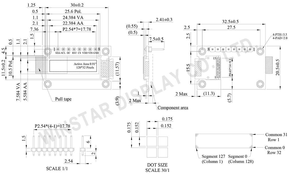
WEA012832D 為一款 0.91 吋熱門尺寸的繪圖型 OLED 顯示模組。與標準 COG 結構WEO012832D不同,此型號採用 COG+PCB 結構,模組背面整合了必要的周邊電路與連接插孔,大幅降低了研發端在硬體整合上的複雜度。
此模組解析度為 128x32 dots,內建 SSD1306BZ 驅動 IC,並透過 4-wire SPI 介面進行通訊。WEA012832D 支援內部 Charge Pump 升壓,開發者可彈性選擇由內部產生顯示驅動電壓或由外部供應 VCC。
| 項目 | 規格 | 單位 |
|---|---|---|
| 點陣(解析度) | 128 x 32 | Dots |
| 模組尺寸 | 32.5 × 20.5 × 2.41 | mm |
| 有效區域 | 22.384 × 5.584 | mm |
| 像素大小 | 0.152 × 0.152 | mm |
| 像素間距 | 0.175 × 0.175 | mm |
| 顯示模式 | 被動矩陣 | |
| 發光顏色 | 單色 | |
| 驅動方式 | 1/32Duty | |
| IC | SSD1306BZ | |
| 介面 | SPI | |
| 尺寸 | 0.91 吋 | |
| 參數 | 符號 | 最小值 | 最大值 | 單位 |
|---|---|---|---|---|
| 邏輯電源電壓 | VDD | 1.65 | 3.3 | V |
| 邏輯電源電壓 | VIN | 4.0 | 6.0 | V |
| 工作溫度 | TOP | -40 | +80 | °C |
| 儲存溫度 | TSTG | -40 | +85 | °C |
| 項目 | 符號 | 條件 | 最小值 | 典型值 | 最大值 | 單位 |
|---|---|---|---|---|---|---|
| 邏輯電源電壓(3V) | VDD | - | 2.8 | 3.0 | 3.3 | V |
| 邏輯電源電壓(5V) | VIN | - | 4.8 | 5.0 | 5.2 | V |
| 輸入高電壓 | VIH | - | 0.8×VDD | - | VDD | V |
| 輸入低電壓 | VIL | - | 0 | - | 0.2×VDD | V |
| 輸出高電壓 | VOH | - | 0.9×VDD | - | VDD | V |
| 輸出低電壓 | VOL | - | 0 | - | 0.1×VDD | V |
| 50% Check Board operating Current | ICC | VDD=3V | - | 13.0 | 26.0 | mA |
| No. | 符號 | 說明 |
|---|---|---|
| 1 | SDA | When serial mode is selected, D1 will be the serial data input SDIN and D0 will be the serial clock input SCLK. |
| 2 | SCL | |
| 3 | DC | Data/Command Control This pin is Data/Command control pin.. When the pin is pulled high and serial interface mode is selected, the data at SDIN is treated as data. When it is pulled low, the data at SDIN will be transferred to the command register. |
| 4 | RST | This pin is reset signal input. When the pin is pulled LOW, initialization of the chip is executed. Keep this pin HIGH (i.e. connect to VDD) during normal operation. |
| 5 | CS | This pin is the chip select input. (active LOW). |
| 6 | VDD | 2.8 ~ 3.3V Power supply pin for core logic operation. |
| 7 | VIN | 4.8 ~ 5.2V Power supply pin for core logic operation. |
| 8 | GND | This is a ground pin. |

通過點擊「允許所有 Cookie」,代表您同意在您的設備上存儲 Cookie 以增強網站瀏覽體驗、分析網站使用情況並協助我們的行銷和網站效能優化工作。您可以在我們的隱私權政策中找到有關於此的更多資訊。