
 – 128x32 I2C SSD1306 - WEA012832F")

우리는 귀하의 프라이버시를 소중히 여깁니다
"모든 쿠키 허용"을 클릭하면 사이트 탐색을 개선하고, 사이트 사용을 분석하며, 마케팅 및 성능 노력에 도움을 주기 위해 쿠키를 귀하의 장치에 저장하는 데 동의한 것으로 간주됩니다. 이 주제에 대한 추가 정보는 당사의 정책에서 확인할 수 있습니다. 개인정보 보호정책

 - WEA012832D")
 - WEA012832D")
 - WEA012832D")
 - WEA012832D")
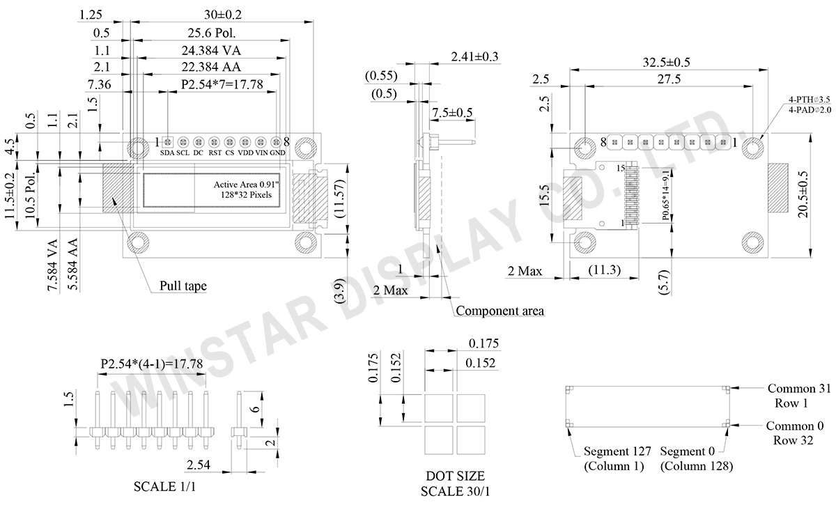
WEA012832D는 하드웨어 구현을 간소화하기 위해 설계된 고집적 0.91인치 그래픽 OLED 디스플레이입니다. 일반적인 COG 구조(WEO012832D 등)와 달리, 본 제품은 COG+PCB 구조를 채택하여 기판 후면에 필수 주변 회로와 핀 헤더를 통합함으로써 개발 복잡성을 최소화했습니다.
SSD1306BZ 컨트롤러가 탑재되어 고속 4-wire SPI 통신을 지원합니다. 또한, 내부 차지 펌프(Charge Pump)를 통한 유연한 전원 설계로 애플리케이션에 따라 내부 승압 구동 또는 외부 VCC 공급 중 최적의 방식을 선택할 수 있습니다.
| 항목 | 치수 | 단위 |
|---|---|---|
| 도트 매트릭스 (해상도) | 128 x 32 | Dots |
| 모듈 치수 | 32.5 × 20.5 × 2.41 | mm |
| 활성 영역 | 22.384 × 5.584 | mm |
| 도트 크기 | 0.152 × 0.152 | mm |
| 도트 피치 | 0.175 × 0.175 | mm |
| 디스플레이 모드 | 패시브 매트릭스 | |
| 디스플레이 색상 | Monochrome | |
| Drive Duty | 1/32Duty | |
| IC | SSD1306BZ | |
| 인터페이스 | SPI | |
| 크기 | 0.91인치 | |
| Parameter | 기호 | 최소값 | 최대값 | 단위 |
|---|---|---|---|---|
| Supply Voltage for Logic | VDD | 1.65 | 3.3 | V |
| Supply Voltage for Logic | VIN | 4.0 | 6.0 | V |
| 작동 온도 | TOP | -40 | +80 | °C |
| 보관 온도 | TSTG | -40 | +85 | °C |
| 항목 | 기호 | 조건 | 최소값 | 대표값 | 최대값 | 단위 |
|---|---|---|---|---|---|---|
| Supply Voltage for Logic(3V) | VDD | - | 2.8 | 3.0 | 3.3 | V |
| Supply Voltage for Logic(5V) | VIN | - | 4.8 | 5.0 | 5.2 | V |
| Input High Volt. | VIH | - | 0.8×VDD | - | VDD | V |
| Input Low Volt. | VIL | - | 0 | - | 0.2×VDD | V |
| Output High Volt. | VOH | - | 0.9×VDD | - | VDD | V |
| Output Low Volt. | VOL | - | 0 | - | 0.1×VDD | V |
| 50% Check Board operating Current | ICC | VDD=3V | - | 13.0 | 26.0 | mA |
| No. | 기호 | 기능 |
|---|---|---|
| 1 | SDA | When serial mode is selected, D1 will be the serial data input SDIN and D0 will be the serial clock input SCLK. |
| 2 | SCL | |
| 3 | DC | Data/Command Control This pin is Data/Command control pin.. When the pin is pulled high and serial interface mode is selected, the data at SDIN is treated as data. When it is pulled low, the data at SDIN will be transferred to the command register. |
| 4 | RST | This pin is reset signal input. When the pin is pulled LOW, initialization of the chip is executed. Keep this pin HIGH (i.e. connect to VDD) during normal operation. |
| 5 | CS | This pin is the chip select input. (active LOW). |
| 6 | VDD | 2.8 ~ 3.3V Power supply pin for core logic operation. |
| 7 | VIN | 4.8 ~ 5.2V Power supply pin for core logic operation. |
| 8 | GND | This is a ground pin. |

"모든 쿠키 허용"을 클릭하면 사이트 탐색을 개선하고, 사이트 사용을 분석하며, 마케팅 및 성능 노력에 도움을 주기 위해 쿠키를 귀하의 장치에 저장하는 데 동의한 것으로 간주됩니다. 이 주제에 대한 추가 정보는 당사의 정책에서 확인할 수 있습니다. 개인정보 보호정책