
私たちはあなたのプライバシーを大切にします
「すべてのクッキーを許可」をクリックすると、サイトのナビゲーションを向上させ、サイト使用状況を分析し、マーケティングおよびパフォーマンスの取り組みを支援するために、クッキーをデバイスに保存することに同意したことになります。この件に関する詳細情報は、ポリシーをご覧ください。プライバシーポリシー

 - WEA012832D")
 - WEA012832D")
 - WEA012832D")
 - WEA012832D")
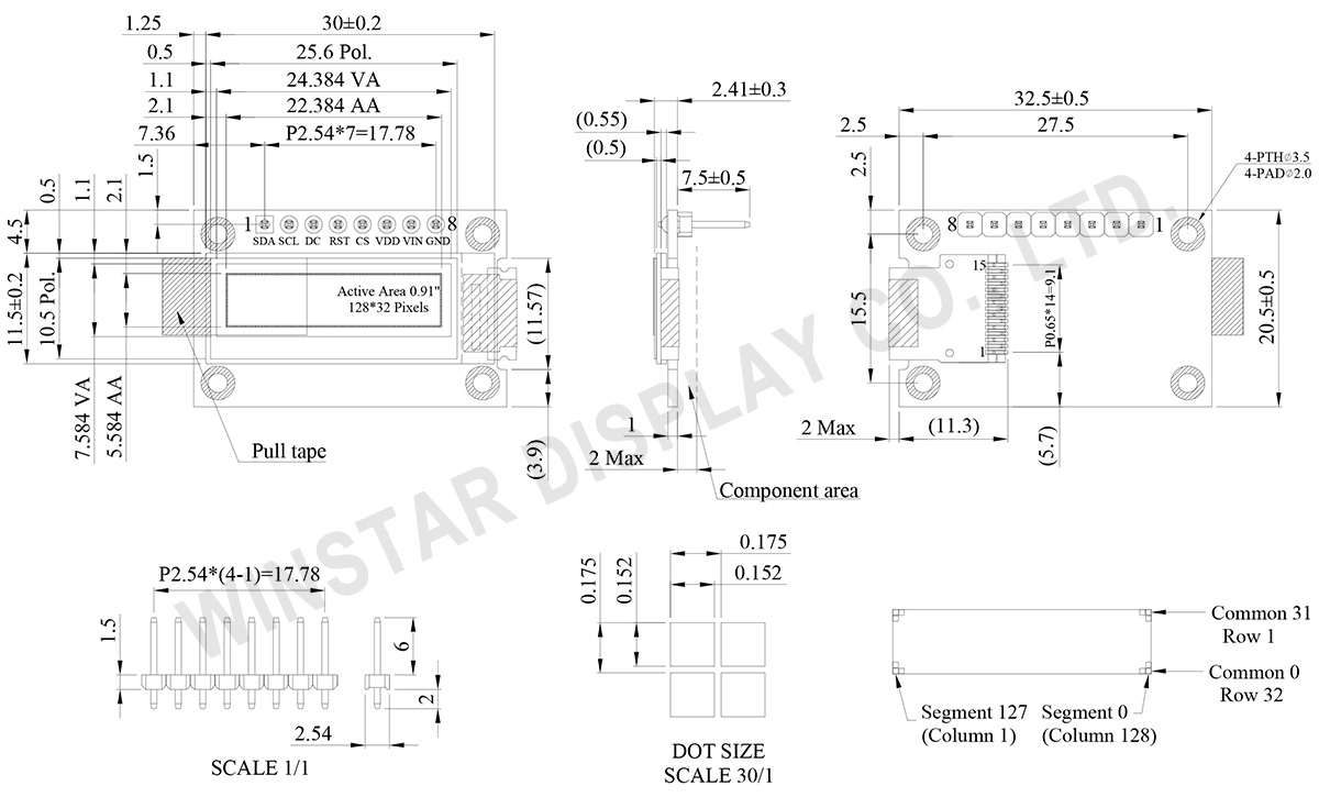
WEA012832Dは、ハードウェアの実装工程を簡略化するために設計された、高集積な0.91インチ・グラフィックOLEDディスプレイです。標準的なCOG構造(WEO012832Dなど)とは異なり、本製品はCOG+PCB構造を採用。基板背面に周辺回路とピンヘッダーを統合しているため、開発工数の削減に大きく貢献します。
コントローラICにはSSD1306BZを採用し、高速な4線式SPI通信に対応しています。また、チャージポンプ内蔵のフレキシブルな電源設計により、内部昇圧による駆動、または外部VCC供給のいずれかをアプリケーションに応じて選択可能です。
| 項目 | 仕様 | 単位 |
|---|---|---|
| ドットマトリックス(解像度) | 128 x 32 | Dots |
| 外形寸法 | 32.5 × 20.5 × 2.41 | mm |
| 有効表示エリア | 22.384 × 5.584 | mm |
| ピクセルサイズ | 0.152 × 0.152 | mm |
| ピクセルピッチ | 0.175 × 0.175 | mm |
| 表示モード | パッシブマトリクス | |
| 発光色 | モノクロ | |
| 駆動方法 | 1/32Duty | |
| IC | SSD1306BZ | |
| インターフェイス | SPI | |
| サイズ | 0.91 インチ | |
| パラメーター | 記号 | 最小値 | 最大値 | 単位 |
|---|---|---|---|---|
| ロジック電源電圧 | VDD | 1.65 | 3.3 | V |
| ロジック電源電圧 | VIN | 4.0 | 6.0 | V |
| 操作温度 | TOP | -40 | +80 | °C |
| 保存温度 | TSTG | -40 | +85 | °C |
| 項目 | 記号 | 条件 | 最小値 | 典型値 | 最大値 | 単位 |
|---|---|---|---|---|---|---|
| ロジック電源電圧(3V) | VDD | - | 2.8 | 3.0 | 3.3 | V |
| ロジック電源電圧(5V) | VIN | - | 4.8 | 5.0 | 5.2 | V |
| 入力電圧(High) | VIH | - | 0.8×VDD | - | VDD | V |
| 入力電圧(Low) | VIL | - | 0 | - | 0.2×VDD | V |
| 出力電圧(High) | VOH | - | 0.9×VDD | - | VDD | V |
| 出力電圧(Low) | VOL | - | 0 | - | 0.1×VDD | V |
| 50% Check Board operating Current | ICC | VDD=3V | - | 13.0 | 26.0 | mA |
| No. | 記号 | 説明 |
|---|---|---|
| 1 | SDA | When serial mode is selected, D1 will be the serial data input SDIN and D0 will be the serial clock input SCLK. |
| 2 | SCL | |
| 3 | DC | Data/Command Control This pin is Data/Command control pin.. When the pin is pulled high and serial interface mode is selected, the data at SDIN is treated as data. When it is pulled low, the data at SDIN will be transferred to the command register. |
| 4 | RST | This pin is reset signal input. When the pin is pulled LOW, initialization of the chip is executed. Keep this pin HIGH (i.e. connect to VDD) during normal operation. |
| 5 | CS | This pin is the chip select input. (active LOW). |
| 6 | VDD | 2.8 ~ 3.3V Power supply pin for core logic operation. |
| 7 | VIN | 4.8 ~ 5.2V Power supply pin for core logic operation. |
| 8 | GND | This is a ground pin. |

「すべてのクッキーを許可」をクリックすると、サイトのナビゲーションを向上させ、サイト使用状況を分析し、マーケティングおよびパフォーマンスの取り組みを支援するために、クッキーをデバイスに保存することに同意したことになります。この件に関する詳細情報は、ポリシーをご覧ください。プライバシーポリシー