– 128x32 I2C SSD1306 - WEA012832F")
私たちはあなたのプライバシーを大切にします
「すべてのクッキーを許可」をクリックすると、サイトのナビゲーションを向上させ、サイト使用状況を分析し、マーケティングおよびパフォーマンスの取り組みを支援するために、クッキーをデバイスに保存することに同意したことになります。この件に関する詳細情報は、ポリシーをご覧ください。プライバシーポリシー


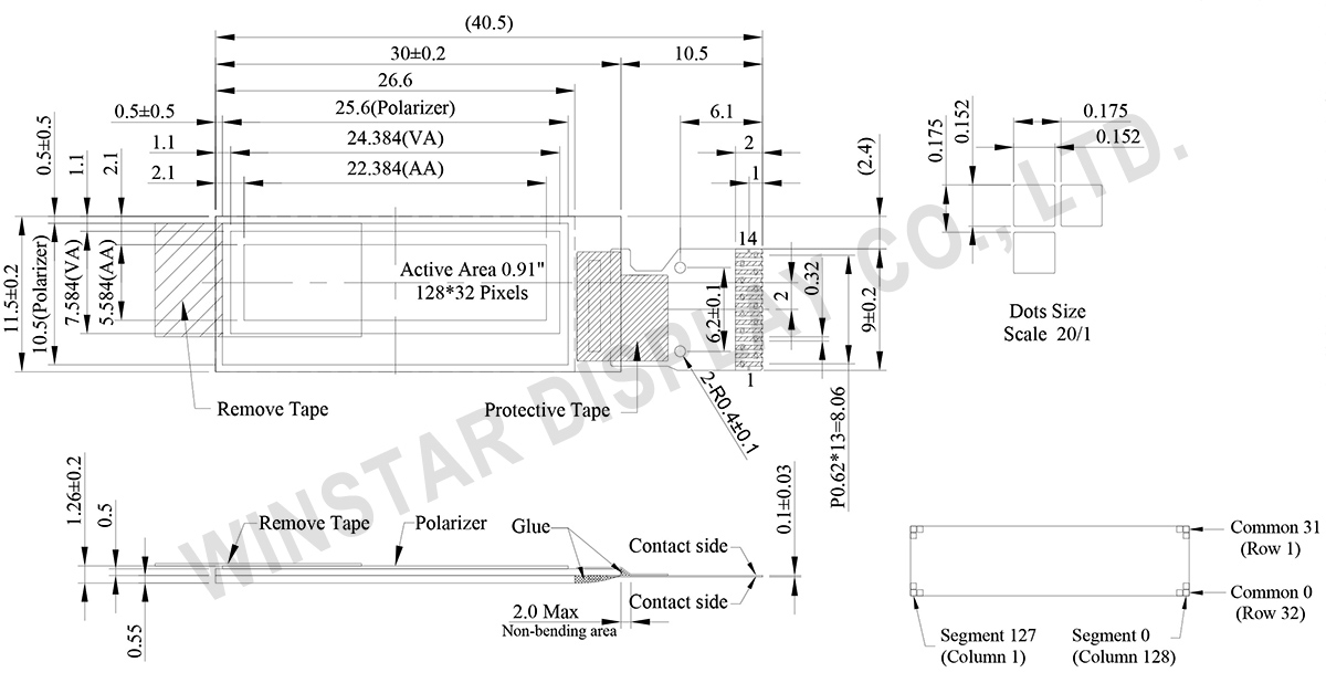
WEO012832FはCOG構造のグラフィックタイプ0.91 OLED I2C ディスプレイです。ウェアラブルに生かせます。 SSD1306 コントロールICを内臓して、I2Cのインターフェースをサポート致します。WEO012832FのAA寸法とVA寸法はWEO012832Dと同じですが、異なるインターフェースとFPCピン配列されております。WEO012832DはSPIのインターフェースをサポート致します。 I2Cのインターフェースを必要する場合、WEO012832Fをご選びください。内部チャージポンプ電源と外部 VCC 電源をサポートしております。
有機EL・COGモジュールは超薄、軽量、高コントラスト、低消費電力、広視野角、高速応答のメリットを有して、壁取付け式デバイス、ハンドヘルド機器、メーター、スマートグリッド、ウェアラブル機器、IoTシステムなどに生かせます。 操作温度範囲は–40℃ to +80℃で、保存温度範囲は -40℃ to +85℃となっております。
| 項目 | 仕様 | 単位 |
|---|---|---|
| ドットマトリックス(解像度) | 128 × 32 | Dots |
| モジュールサイズ | 30.0 × 11.5 × 1.26 | mm |
| 有効エリア | 22.384 × 5.584 | mm |
| ピクセルサイズ | 0.152 × 0.152 | mm |
| ピクセルピッチ | 0.175 × 0.175 | mm |
| 表示モード | Passive Matrix パッシブマトリクス | |
| 発光色 | モノクロ | |
| 駆動方法 | 1/32 Duty | |
| IC | SSD1306 | |
| インターフェイス | I2C | |
| サイズ (対角線) | 0.91 インチ | |
| パラメーター | 記号 | 最小値 | 最大値 | 単位 |
|---|---|---|---|---|
| ロジック電源電圧 | VDD | 0 | 4.0 | V |
| Display電源電圧 | VCC | 0 | 16.0 | V |
| 操作温度 | TOP | -40 | +80 | °C |
| 保存温度 | TSTG | -40 | +85 | °C |
| 項目 | 記号 | 条件 | 最小値 | 典型値 | 最大値 | 単位 |
|---|---|---|---|---|---|---|
| ロジック電源電圧 | VDD | - | 2.8 | 3.0 | 3.3 | V |
| Display電源電圧 | VCC | - | 7 | 7.25 | 8 | V |
| 高レベル入力 | VIH | - | 0.8×VDD | - | VDDIO | V |
| 低レベル入力 | VIL | - | 0 | - | 0.2×VDD | V |
| 高レベル出力 | VOH | - | 0.9×VDD | - | VDDIO | V |
| 低レベル出力 | VOL | - | 0 | - | 0.1×VDD | V |
| VCC 動作電流 (VCC Supplied Externally) | ICC | Vcc =7.25V | - | 7 | 11 | mA |
| No. | 記号 | 功能説明 |
|---|---|---|
| 1 | C2P | Positive Terminal of the Flying Inverting CapacitorNegative Terminal of the Flying Boost CapacitorThe charge-pump capacitors are required between the terminals. They must be floated when the converter is not used. |
| 2 | C2N | |
| 3 | C1P | |
| 4 | C1N | |
| 5 | VBAT | Power Supply for DC/DC Converter Circuit This is the power supply pin for the internal buffer of the DC/DC voltage converter. It must be connected to external source when the converter is used. It should be connected to VDD when the converter is not used. |
| 6 | NC | No connection |
| 7 | VSS | Ground of Logic Circuit This is a ground pin. It acts as a reference for the logic pins. It must be connected to external ground. |
| 8 | VDD | Power Supply for Logic This is a voltage supply pin. It must be connected to external source. |
| 9 | RES# | Power Reset for Controller and Driver This pin is reset signal input. When the pin is low, initialization of the chip is executed. |
| 10 | SCL | I2C mode is selected, D2, D1 should be tied together and serve as SDAout, SDAin inapplication and D0 is the serial clock input, SCL. |
| 11 | SDA | |
| 12 | IREF | Current Reference for Brightness Adjustment This pin is segment current reference pin. A resistor should be connected between this pin and VSS. Set the current lower than 12.5μA. |
| 13 | VCOMH | Voltage Output High Level for COM Signal This pin is the input pin for the voltage output high level for COM signals. A capacitor should be connected between this pin and VSS. |
| 14 | VCC | Power Supply for OEL Panel This is the most positive voltage supply pin of the chip. A stabilization capacitor should be connected between this pin and VSS when the converter is used. It must be connected to external source when the converter is not used. |

「すべてのクッキーを許可」をクリックすると、サイトのナビゲーションを向上させ、サイト使用状況を分析し、マーケティングおよびパフォーマンスの取り組みを支援するために、クッキーをデバイスに保存することに同意したことになります。この件に関する詳細情報は、ポリシーをご覧ください。プライバシーポリシー