Display OLED 128x32 I2C Compacto e Eficiente
O WEO012832F da Winstar é um display OLED 128x32 I2C compacto e de alto desempenho, ideal para uma ampla variedade de aplicações, incluindo dispositivos vestíveis, instrumentos portáteis e sistemas IoT. Com um tamanho diagonal de apenas 0,91 polegadas, este display OLED gráfico oferece excelente clareza e uma alta taxa de contraste, tornando-o perfeito para dispositivos compactos que exigem desempenho visual nítido.
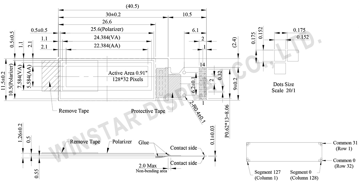
Projetado com o controlador SSD1306, o WEO012832F suporta a interface I2C, oferecendo um método de comunicação simples e confiável. Este módulo de display opera com baixo consumo de energia, tornando-o adequado para dispositivos alimentados por bateria e aplicações que exigem eficiência energética. O módulo possui um conector FPC de 14 pinos e pode ser alimentado por uma fonte de 3V, suportando tanto o fornecimento interno por bomba de carga quanto a opção de VCC externo.
Comparado ao modelo WEO012832D, o WEO012832F tem uma configuração de pinos diferente, mas mantém as mesmas dimensões mecânicas compactas. Este display é leve, fácil de integrar e suporta uma faixa de temperatura de operação de -40℃ a +80℃, com temperaturas de armazenamento de -40℃ a +85℃, garantindo confiabilidade em diversos ambientes.
O WEO012832F está disponível em três cores: Branco, Amarelo e Azul Claro, oferecendo opções de display versáteis para várias aplicações, incluindo sistemas de automação residencial, dispositivos médicos, displays automotivos e sistemas de monitoramento de energia. Sua pequena pegada e desempenho eficiente fazem dele a escolha ideal para projetos em que o espaço é limitado, mas a qualidade do display é essencial.
Principais Características
- Resolução de matriz de pontos 128x32 para visuais claros e detalhados
- Baixo consumo de energia com interface I2C
- Tamanho compacto de 0,91 polegadas de diagonal
- Controlador SSD1306 integrado para desempenho confiável
- Faixa de temperatura: de -40℃ a +80℃ para operação, de -40℃ a +85℃ para armazenamento
- Suporta opções de cor Branco, Amarelo e Azul Claro
- Ideal para dispositivos vestíveis, automação residencial, IoT e muito mais
Aplicações
- Dispositivos vestíveis e sistemas de monitoramento de saúde
- Displays para automação residencial e medidores inteligentes
- Sistemas Cloud e IoT
- Instrumentos portáteis e dispositivos eletrônicos
- Displays de painéis automotivos e sistemas energéticos