 – 128x32 I2C SSD1306 - WEA012832F")
我們重視您的隱私
通過點擊「允許所有 Cookie」,代表您同意在您的設備上存儲 Cookie 以增強網站瀏覽體驗、分析網站使用情況並協助我們的行銷和網站效能優化工作。您可以在我們的隱私權政策中找到有關於此的更多資訊。


WEO012832F是一款128x32 COG 繪圖型0.91吋小尺寸單色PMOLED 模組,非常適用於穿戴式裝置顯示器。WEO012832F內建SSD1306 控制器IC,模組支援I2C介面,此款OLED面板外觀尺寸、AA區及VA區尺寸與WEO012832D相同,但是兩款的FPC pin數及出pin方式與interface介面不相同,WEO012832D是僅能使用SPI串列式介面,如需使用I2C interface請選用WEO012832F此款模組。此型號OLED模組可支援內部升壓及外部供電。
WEO012832F為COG OLED模組,特點是重量輕薄、高對比、低耗電、廣視角、反應速度快,適用於牆面型(wall devices) 或手持式測量儀器(meter devices)、智能科技與智慧能源系統、物聯網設備、智慧電表、醫療儀器以及穿戴式裝置、電子菸等等。WEO012832F模組的工作溫度是-40℃至+80℃,儲存溫度-40℃至+85℃ 。
| 項目 | 規格 | 單位 |
|---|---|---|
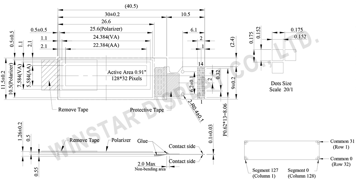
| 點陣(解析度) | 128 × 32 | Dots |
| 模組尺寸 | 30.0 × 11.5 × 1.26 | mm |
| 有效區域 | 22.384 × 5.584 | mm |
| 像素大小 | 0.152 × 0.152 | mm |
| 像素間距 | 0.175 × 0.175 | mm |
| 顯示模式 | Passive Matrix 被動矩陣 | |
| 發光顏色 | 單色 | |
| 驅動方式 | 1/32 Duty | |
| IC | SSD1306 | |
| 介面 | I2C | |
| 尺寸(對角線) | 0.91 吋 | |
| 參數 | 符號 | 最小值 | 最大值 | 單位 |
|---|---|---|---|---|
| 邏輯電源電壓 | VDD | 0 | 4.0 | V |
| 顯示電源電壓 | VCC | 0 | 16.0 | V |
| 工作溫度 | TOP | -40 | +80 | °C |
| 儲存溫度 | TSTG | -40 | +85 | °C |
| 項目 | 符號 | 條件 | 最小值 | 典型值 | 最大值 | 單位 |
|---|---|---|---|---|---|---|
| 邏輯電源電壓 | VDD | - | 2.8 | 3.0 | 3.3 | V |
| 顯示電源電壓 | VCC | - | 7 | 7.25 | 8 | V |
| 輸入高準位 | VIH | - | 0.8×VDD | - | VDDIO | V |
| 輸入低準位 | VIL | - | 0 | - | 0.2×VDD | V |
| 輸出高準位 | VOH | - | 0.9×VDD | - | VDDIO | V |
| 輸出低準位 | VOL | - | 0 | - | 0.1×VDD | V |
| VCC的工作電流 (VCC Supplied Externally) | ICC | Vcc =7.25V | - | 7 | 11 | mA |
| No. | 符號 | 功能說明 |
|---|---|---|
| 1 | C2P | Positive Terminal of the Flying Inverting CapacitorNegative Terminal of the Flying Boost CapacitorThe charge-pump capacitors are required between the terminals. They must be floated when the converter is not used. |
| 2 | C2N | |
| 3 | C1P | |
| 4 | C1N | |
| 5 | VBAT | Power Supply for DC/DC Converter Circuit This is the power supply pin for the internal buffer of the DC/DC voltage converter. It must be connected to external source when the converter is used. It should be connected to VDD when the converter is not used. |
| 6 | NC | No connection |
| 7 | VSS | Ground of Logic Circuit This is a ground pin. It acts as a reference for the logic pins. It must be connected to external ground. |
| 8 | VDD | Power Supply for Logic This is a voltage supply pin. It must be connected to external source. |
| 9 | RES# | Power Reset for Controller and Driver This pin is reset signal input. When the pin is low, initialization of the chip is executed. |
| 10 | SCL | I2C mode is selected, D2, D1 should be tied together and serve as SDAout, SDAin inapplication and D0 is the serial clock input, SCL. |
| 11 | SDA | |
| 12 | IREF | Current Reference for Brightness Adjustment This pin is segment current reference pin. A resistor should be connected between this pin and VSS. Set the current lower than 12.5μA. |
| 13 | VCOMH | Voltage Output High Level for COM Signal This pin is the input pin for the voltage output high level for COM signals. A capacitor should be connected between this pin and VSS. |
| 14 | VCC | Power Supply for OEL Panel This is the most positive voltage supply pin of the chip. A stabilization capacitor should be connected between this pin and VSS when the converter is used. It must be connected to external source when the converter is not used. |

通過點擊「允許所有 Cookie」,代表您同意在您的設備上存儲 Cookie 以增強網站瀏覽體驗、分析網站使用情況並協助我們的行銷和網站效能優化工作。您可以在我們的隱私權政策中找到有關於此的更多資訊。