
我们重视您的隐私
通过点击「允许所有 Cookie」,代表您同意在您的设备上存储 Cookie 以增强网站浏览体验、分析网站使用情况并协助我们的营销和网站效能优化工作。您可以在我们的隐私权政策中找到有关于此的更多信息。
 - WEA012832D")
 - WEA012832D")
 - WEA012832D")
 - WEA012832D")
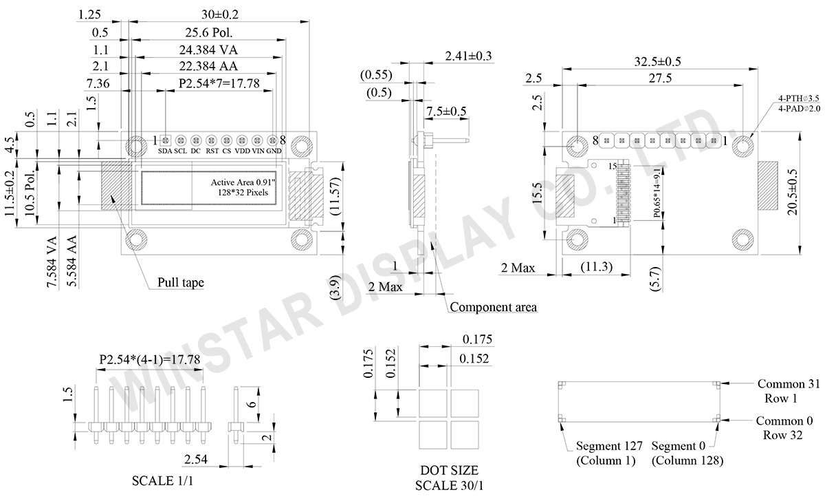
WEA012832D 是一款高集成度的 0.91 英寸绘图型 OLED 显示模组,专为简化硬件设计而生。与传统的 COG 结构(如 WEO012832D)不同,该型号采用 COG+PCB 结构,模组背面集成了必要的外部电路与排针接口,显著降低了研发端的硬件整合难度。
此模组分辨率为 128x32 dots,内置 SSD1306BZ 驱动 IC,通过 4线 SPI 接口进行通讯。WEA012832D 内部集成 Charge Pump(电荷泵)升压电路,开发者可灵活选择内部升压驱动或外部供应 VCC,优化整机功耗管理。
| 项目 | 规格 | 单位 |
|---|---|---|
| 点阵(分辨率) | 128 x 32 | Dots |
| 模块尺寸 | 32.5 × 20.5 × 2.41 | mm |
| 有效区域 | 22.384 × 5.584 | mm |
| 像素大小 | 0.152 × 0.152 | mm |
| 像素间距 | 0.175 × 0.175 | mm |
| 显示模式 | 被动矩阵 | |
| 发光颜色 | 单色 | |
| 驱动方式 | 1/32Duty | |
| IC | SSD1306BZ | |
| 接口 | SPI | |
| 尺寸 | 0.91 寸 | |
| 参数 | 符号 | 最小值 | 最大值 | 单位 |
|---|---|---|---|---|
| 逻辑电源电压 | VDD | 1.65 | 3.3 | V |
| 逻辑电源电压 | VIN | 4.0 | 6.0 | V |
| 工作温度 | TOP | -40 | +80 | °C |
| 储存温度 | TSTG | -40 | +85 | °C |
| 项目 | 符号 | 条件 | 最小值 | 典型值 | 最大值 | 单位 |
|---|---|---|---|---|---|---|
| 逻辑电源电压(3V) | VDD | - | 2.8 | 3.0 | 3.3 | V |
| 逻辑电源电压(5V) | VIN | - | 4.8 | 5.0 | 5.2 | V |
| 输入高电压 | VIH | - | 0.8×VDD | - | VDD | V |
| 输入低电压 | VIL | - | 0 | - | 0.2×VDD | V |
| 输出高电压 | VOH | - | 0.9×VDD | - | VDD | V |
| 输出低电压 | VOL | - | 0 | - | 0.1×VDD | V |
| 50% Check Board operating Current | ICC | VDD=3V | - | 13.0 | 26.0 | mA |
| No. | 符号 | 说明 |
|---|---|---|
| 1 | SDA | When serial mode is selected, D1 will be the serial data input SDIN and D0 will be the serial clock input SCLK. |
| 2 | SCL | |
| 3 | DC | Data/Command Control This pin is Data/Command control pin.. When the pin is pulled high and serial interface mode is selected, the data at SDIN is treated as data. When it is pulled low, the data at SDIN will be transferred to the command register. |
| 4 | RST | This pin is reset signal input. When the pin is pulled LOW, initialization of the chip is executed. Keep this pin HIGH (i.e. connect to VDD) during normal operation. |
| 5 | CS | This pin is the chip select input. (active LOW). |
| 6 | VDD | 2.8 ~ 3.3V Power supply pin for core logic operation. |
| 7 | VIN | 4.8 ~ 5.2V Power supply pin for core logic operation. |
| 8 | GND | This is a ground pin. |

通过点击「允许所有 Cookie」,代表您同意在您的设备上存储 Cookie 以增强网站浏览体验、分析网站使用情况并协助我们的营销和网站效能优化工作。您可以在我们的隐私权政策中找到有关于此的更多信息。