


 - WEO012832N")
우리는 귀하의 프라이버시를 소중히 여깁니다
"모든 쿠키 허용"을 클릭하면 사이트 탐색을 개선하고, 사이트 사용을 분석하며, 마케팅 및 성능 노력에 도움을 주기 위해 쿠키를 귀하의 장치에 저장하는 데 동의한 것으로 간주됩니다. 이 주제에 대한 추가 정보는 당사의 정책에서 확인할 수 있습니다. 개인정보 보호정책


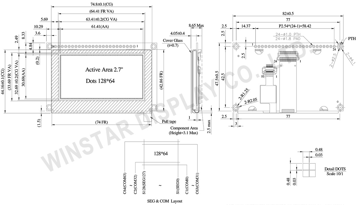
모델 번호 WEP012864Q-CTP
►유형 : 그래픽
►구조 : COG + 프레임 + PCB
►크기 : 2.7 인치
►128 x 64 점 행렬
►IC:SSD1309
►3V 전원 공급 장치
►1/64 duty
►인터페이스 : 6800, 8080, SPI, I2C
►용량식 터치패널(스크린)이 있는(CTP)
►터치포인트 : 1 손가락
►디스플레이 색상: 백색 / 노란색 / 하늘색 / 녹색
WEP012864Q-CTP 모델은 128x64 픽셀로 구성된 2.7인치 대각선 크기의 COG 그래픽 OLED로, 용량성 터치 패널이 내장되어 있습니다. 이 OLED 모듈은 SSD1309 IC가 내장되어 있으며, 6800/8080 8비트 병렬, I2C 및 4-Wire SPI 인터페이스를 지원하며, 로직용 공급 전압은 3V입니다. 50% 체크 보드 전류로 175mA @3.0V VDD(일반 값), 드라이빙 듀티 1/64를 갖추고 있습니다. 이 모델은 모듈에 용량성 터치 패널이 내장되어 있으며, I2C 인터페이스를 지원하는 GT911 IC가 내장되어 있으며 CTP용 하나의 감지 포인트를 갖추고 있습니다. 또한 일반적인 반사 유리 표면이 있습니다. 이 모듈에는 고객이 와이어 연결을 사용할 수 있도록 모듈에 PCB 보드가 있으며, 고객은 응용 프로그램에 대한 추가 PCB를 개발할 필요가 없습니다. 또한 VCC 회로를 PCB에 통합하여 고객이 사용하기 쉽게하였습니다.
WEP012864Q-CTP 모델은 모듈에 PCB가 있는 COG OLED 디스플레이입니다. 이 PCB 보드에는 네 개의 마운팅 홀이 있어 고객이 응용 프로그램에 모듈을 고정하는 데 사용하기 쉬운 방법입니다. 이 OLED 모듈은 스마트 홈 응용 프로그램, 의료 기기, 산업 제어 등에 적합합니다. WEP012864Q-CTP 모델은 -20℃에서 +70℃까지의 온도에서 작동할 수 있으며, 저장 온도는 -30℃에서 +80℃로 범위가 있습니다./p>
Data source ref: WEP012864QWPP3D00000
| 항목 | 치수 | 단위 |
|---|---|---|
| 도트 매트릭스 | 128 x 64 | - |
| 모듈 치수 | 82.0 × 47.5 × 8.65 Max. | mm |
| 활성 영역 | 61.41 × 30.69 | mm |
| 도트 크기 | 0.45 × 0.45 | mm |
| 도트 피치 | 0.48 × 0.48 | mm |
| 디스플레이 모드 | 패시브 매트릭스 (Passive Matrix) | |
| 디스플레이 색 | Monochrome | |
| Drive Duty | 1/64 Duty | |
| IC | SSD1309 | |
| 인터페이스 | 6800,8080,4-Wire SPI,I2C | |
| 크기 | 2.7 인치 | |
| CTP IC | GT911 | |
| 터치포인트 | 1 | |
| CTP 인터페이스 | I2C | |
| 표면 | 눈부심 | |
| Parameter | 기호 | 최소값 | 최대값 | 단위 |
|---|---|---|---|---|
| Supply Voltage for Logic | VDD | -0.3 | 4 | V |
| 작동 온도 | TOP | -20 | +70 | °C |
| 보관 온도 | TSTG | -30 | +80 | °C |
| 항목 | 기호 | 조건 | 최소값 | 대표값 | 최대값 | 단위 |
|---|---|---|---|---|---|---|
| Supply Voltage for Logic | VDD | - | 2.8 | 3.0 | 3.3 | V |
| High Level Input | VIH | - | 0.8×VDD | - | - | V |
| Low Level Input | VIL | - | - | - | 0.2×VDD | V |
| High Level Output | VOH | - | 0.9×VDD | - | - | V |
| Low Level Output | VOL | - | - | - | 0.1×VDD | V |
| 50% Check Board operating Current | VDD =3V | - | 175 | 350 | mA | |
| 항목 | 기호 | 최소값 | 대표값 | 최대값 | 단위 |
|---|---|---|---|---|---|
| Input High Volt. | VIH | 0.75xVDD | VDD+0.3 | V | |
| Input Low Volt. | VIL | -0.3 | - | 0.25xVDD | V |
| Output High Volt. | VOH | 0.85xVDD | - | - | V |
| Output Low Volt. | VOL | - | - | 0.15xVDD | V |
| No. | 기호 | 기능 | |||||||||||||||
|---|---|---|---|---|---|---|---|---|---|---|---|---|---|---|---|---|---|
| 1 | VSS | Ground. | |||||||||||||||
| 2 | VDD | Power supply pin for core logic operation | |||||||||||||||
| 3 | NC | No connection | |||||||||||||||
| 4 | D/C# | This pin is Data/Command control pin connecting to the MCU. When the pin is pulled HIGH, the data at D[7:0] will be interpreted as data. When the pin is pulled LOW, the data at D[7:0] will be transferred to a command register. In I2C mode, this pin acts as SA0 for slave address selection. |
|||||||||||||||
| 5 | R/W# (WR#) |
This pin is read / write control input pin connecting to the MCU interface. When 6800 interface mode is selected, this pin will be used as Read/Write (R/W#) selection input. Read mode will be carried out when this pin is pulled HIGH and write mode when LOW. When 8080 interface mode is selected, this pin will be the Write (WR#) input. Data write operation is initiated when this pin is pulled LOW and the chip is selected. When serial or I2C interface is selected, this pin must be connected to VSS. |
|||||||||||||||
| 6 | E(/RD#) | This pin is MCU interface input. When 6800 interface mode is selected, this pin will be used as the Enable (E) signal. Read/write operation is initiated when this pin is pulled HIGH and the chip is selected. When 8080 interface mode is selected, this pin receives the Read (RD#) signal. Read operation is initiated when this pin is pulled LOW and the chip is selected. When serial or I2C interface is selected, this pin must be connected to VSS. |
|||||||||||||||
| 7-14 | D0~D7 | These pins are bi-directional data bus connecting to the MCU data bus. Unused pins are recommended to tie LOW. When serial interface mode is selected, D0 will be the serial clock input: SCLK; D1 will be the serial data input: SDIN and D2 should be kept NC. When I2C mode is selected, D2, D1 should be tied together and serve as SDAout, SDAin in application and D0 is the serial clock input, SCL. |
|||||||||||||||
| 15 | NC | No connection | |||||||||||||||
| 16 | RES# | This pin is reset signal input. When the pin is pulled LOW, initialization of the chip is executed. Keep this pin pull HIGH during normal operation. |
|||||||||||||||
| 17 | CS# | This pin is the chip select input connecting to the MCU. The chip is enabled for MCU communication only when CS# is pulled LOW (active LOW). |
|||||||||||||||
| 18 | NC | No connection | |||||||||||||||
| 19 | BS2 | MCU bus interface selection pins. Select appropriate logic setting as described in the following table. BS2 and BS1 are pin select
(1) 0 is connected to VSS (2) 1 is connected to VDD |
|||||||||||||||
| 20 | BS1 | ||||||||||||||||
| 21 | TP_SCK | I2C clock signal | |||||||||||||||
| 22 | TP_SDA | I2C data signal | |||||||||||||||
| 23 | TP_INT | External interrupt signal, active low | |||||||||||||||
| 24 | TP_RST | External reset signal, active low |

"모든 쿠키 허용"을 클릭하면 사이트 탐색을 개선하고, 사이트 사용을 분석하며, 마케팅 및 성능 노력에 도움을 주기 위해 쿠키를 귀하의 장치에 저장하는 데 동의한 것으로 간주됩니다. 이 주제에 대한 추가 정보는 당사의 정책에서 확인할 수 있습니다. 개인정보 보호정책