


私たちはあなたのプライバシーを大切にします
「すべてのクッキーを許可」をクリックすると、サイトのナビゲーションを向上させ、サイト使用状況を分析し、マーケティングおよびパフォーマンスの取り組みを支援するために、クッキーをデバイスに保存することに同意したことになります。この件に関する詳細情報は、ポリシーをご覧ください。プライバシーポリシー


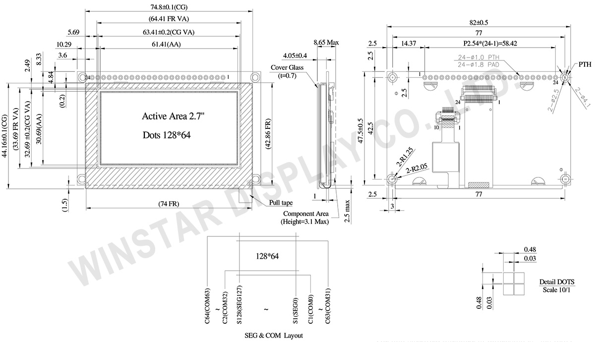
型番 WEP012864Q-CTP
►タイプ: グラフィック有機ELディスプレイ
►結構: COG + 鉄フレーム + PCB
►サイズ: 2.7インチ
►128 x 64 ドットマトリックス
►IC:SSD1309
►3V電源電圧
►1/64 duty
►インターフェース: 6800, 8080, SPI, I2C
►静電容量式タッチパネル(CTP)
►検出ポイント: 1
►発光色: 白色 / 黄色 / 空色 / 緑色
WEP012864Q-CTP モジュールはCOG構造の グラフィック有機EL ディスプレイで、 対角寸法は 2.7 インチで、解像度は128x64です。 SSD1309 ICを内蔵し、6800/8080 8ビットのパラレル、I2Cと 4線式SPIインターフェースをサポート致します。ロジックの電源電圧は3Vで、50%チェックボード電流での表示は175mA @3.0V VDD (標準値)で、駆動デューティは 1/64です。このモジュールは 静電容量式タッチパネルを搭載しており、GT911 IC を内蔵し、I2C インターフェースをサポート致します。 1本指で検出ポイントをサポートし、表面ガラスが通常のグレアタイプです。 WEP012864Q-CTP モジュールはPCB基板を搭載しており、 お得意先の設備と製品にワイヤーで接続することができます。そして、PCB基板にVCC回路が設けられており、固定用の取り付け穴も付きのため 、お得意先の開発及び作業の効率を向上させます。
この有機ELディスプレイはスマートホームアプリケーション、医療機器 、産業用制御システム などに適しております。 操作温度範囲は-20℃ ~ +70℃で、保存温度範囲は -30℃ ~ +80℃です。
Data source ref: WEP012864QWPP3D00000
| 項目 | 仕様 | 単位 |
|---|---|---|
| ドットマトリックス(解像度) | 128 x 64 | - |
| モジュールサイズ | 82.0 × 47.5 × 8.65 Max. | mm |
| 有効エリア | 61.41 × 30.69 | mm |
| ドットサイズ | 0.45 × 0.45 | mm |
| ドットピッチ | 0.48 × 0.48 | mm |
| 表示モード | パッシブマトリクス | |
| 発光色 | モノクロ | |
| 駆動方法 | 1/64 Duty | |
| IC | SSD1309 | |
| インターフェイス | 6800,8080,4-Wire SPI,I2C | |
| 表示サイズ | 2.7インチ | |
| CTP IC | GT911 | |
| 検出ポイント | 1 | |
| CTP インターフェイス | I2C | |
| 表面処理 | グレア | |
| パラメーター | 記号 | 最小値 | 最大値 | 単位 |
|---|---|---|---|---|
| ロジック電源電圧 | VDD | -0.3 | 4 | V |
| 操作温度 | TOP | -20 | +70 | °C |
| 保存温度 | TSTG | -30 | +80 | °C |
| 項目 | 記号 | 条件 | 最小値 | 典型値 | 最大値 | 単位 |
|---|---|---|---|---|---|---|
| ロジック電源電圧 | VDD | - | 2.8 | 3.0 | 3.3 | V |
| 高レベル入力 | VIH | - | 0.8×VDD | - | - | V |
| 低レベル入力 | VIL | - | - | - | 0.2×VDD | V |
| 高レベル出力 | VOH | - | 0.9×VDD | - | - | V |
| 低レベル出力 | VOL | - | - | - | 0.1×VDD | V |
| 50% Check Board operating Current | VDD =3V | - | 175 | 350 | mA | |
| 項目 | 記号 | 最小値 | 典型値 | 最大値 | 単位 |
|---|---|---|---|---|---|
| 高レベル入力 | VIH | 0.75xVDD | VDD+0.3 | V | |
| 低レベル入力 | VIL | -0.3 | - | 0.25xVDD | V |
| 高レベル出力 | VOH | 0.85xVDD | - | - | V |
| 低レベル出力 | VOL | - | - | 0.15xVDD | V |
| No. | 記号 | 説明 | |||||||||||||||
|---|---|---|---|---|---|---|---|---|---|---|---|---|---|---|---|---|---|
| 1 | VSS | Ground. | |||||||||||||||
| 2 | VDD | Power supply pin for core logic operation | |||||||||||||||
| 3 | NC | No connection | |||||||||||||||
| 4 | D/C# | This pin is Data/Command control pin connecting to the MCU. When the pin is pulled HIGH, the data at D[7:0] will be interpreted as data. When the pin is pulled LOW, the data at D[7:0] will be transferred to a command register. In I2C mode, this pin acts as SA0 for slave address selection. |
|||||||||||||||
| 5 | R/W# (WR#) |
This pin is read / write control input pin connecting to the MCU interface. When 6800 interface mode is selected, this pin will be used as Read/Write (R/W#) selection input. Read mode will be carried out when this pin is pulled HIGH and write mode when LOW. When 8080 interface mode is selected, this pin will be the Write (WR#) input. Data write operation is initiated when this pin is pulled LOW and the chip is selected. When serial or I2C interface is selected, this pin must be connected to VSS. |
|||||||||||||||
| 6 | E(/RD#) | This pin is MCU interface input. When 6800 interface mode is selected, this pin will be used as the Enable (E) signal. Read/write operation is initiated when this pin is pulled HIGH and the chip is selected. When 8080 interface mode is selected, this pin receives the Read (RD#) signal. Read operation is initiated when this pin is pulled LOW and the chip is selected. When serial or I2C interface is selected, this pin must be connected to VSS. |
|||||||||||||||
| 7-14 | D0~D7 | These pins are bi-directional data bus connecting to the MCU data bus. Unused pins are recommended to tie LOW. When serial interface mode is selected, D0 will be the serial clock input: SCLK; D1 will be the serial data input: SDIN and D2 should be kept NC. When I2C mode is selected, D2, D1 should be tied together and serve as SDAout, SDAin in application and D0 is the serial clock input, SCL. |
|||||||||||||||
| 15 | NC | No connection | |||||||||||||||
| 16 | RES# | This pin is reset signal input. When the pin is pulled LOW, initialization of the chip is executed. Keep this pin pull HIGH during normal operation. |
|||||||||||||||
| 17 | CS# | This pin is the chip select input connecting to the MCU. The chip is enabled for MCU communication only when CS# is pulled LOW (active LOW). |
|||||||||||||||
| 18 | NC | No connection | |||||||||||||||
| 19 | BS2 | MCU bus interface selection pins. Select appropriate logic setting as described in the following table. BS2 and BS1 are pin select
(1) 0 is connected to VSS (2) 1 is connected to VDD |
|||||||||||||||
| 20 | BS1 | ||||||||||||||||
| 21 | TP_SCK | I2C clock signal | |||||||||||||||
| 22 | TP_SDA | I2C data signal | |||||||||||||||
| 23 | TP_INT | External interrupt signal, active low | |||||||||||||||
| 24 | TP_RST | External reset signal, active low |

「すべてのクッキーを許可」をクリックすると、サイトのナビゲーションを向上させ、サイト使用状況を分析し、マーケティングおよびパフォーマンスの取り組みを支援するために、クッキーをデバイスに保存することに同意したことになります。この件に関する詳細情報は、ポリシーをご覧ください。プライバシーポリシー