


 - WEA012864AA")
")
私たちはあなたのプライバシーを大切にします
「すべてのクッキーを許可」をクリックすると、サイトのナビゲーションを向上させ、サイト使用状況を分析し、マーケティングおよびパフォーマンスの取り組みを支援するために、クッキーをデバイスに保存することに同意したことになります。この件に関する詳細情報は、ポリシーをご覧ください。プライバシーポリシー


WinstarのWEO012864Qは2.7インチ、128x64ドットのOLEDディスプレイモジュールです。このグラフィックディスプレーはSSD1309コントローラーICが内蔵し、インターフェースが6800/8080 8-bit、I2C及び 4線式シリアルが使用でき、3V電源のモジュールです。WEO012864Qのモジュール寸法は73.0 x 41.86 mmで、アクティブエリアサイズは61.41x30.69mmです。このアイテムはOLEDパネルWEO012864Kと同じく30ぴんFPCがあり、FPCのピン割り当てはWEX012864L(30ピン)と同じに定義されています。
WEO012864QはCOG構造のOLEDディスプレイです。このアイテムは軽量で、低消費電力で、超薄型です。このOLEDモジュールは壁/メーター機器、家庭用アプリケーション、POSシステム、クラウド/IoTシステム、インテリジェンステクノロジデバイス、エネルギーシステム、通信システム、医療器械などに適しています。WEO012864Q OLEDモジュールの動作可能の温度範囲は-40℃〜+80℃、保存温度範囲は-40℃〜+85℃です。このアイテムの標準発光色は黄色、白色とスカイブルーで利用できます。
 Frame Option
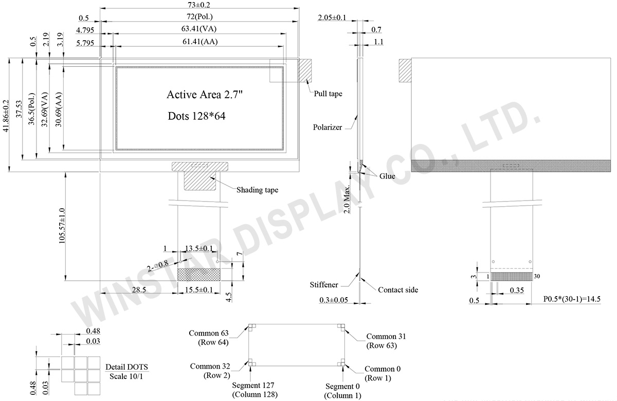
| 項目 | 仕様 | 単位 |
|---|---|---|
| ドットマトリックス(解像度) | 128 x 64 | - |
| モジュールサイズ | 73.0 × 41.86 × 2.05 | mm |
| 有効エリア | 61.41 × 30.69 | mm |
| ドットサイズ | 0.45 × 0.45 | mm |
| ドットピッチ | 0.48 × 0.48 | mm |
| 表示モード | 被动矩阵 | |
| 発光色 | 单色 | |
| 駆動方法 | 1/64 Duty | |
| IC | SSD1309 | |
| インターフェイス | I2C, 4-Wire SPI ,6800, 8080 | |
| 表示サイズ(対角線) | 2.7 インチ | |
| パラメーター | 記号 | 最小値 | 最大値 | 単位 |
|---|---|---|---|---|
| ロジック電源電圧 | VDD | -0.3 | 4 | V |
| Display電源電圧 | VCC | 0 | 15 | V |
| 操作温度 | TOP | -40 | +80 | °C |
| 保存温度 | TSTG | -40 | +85 | °C |
| 項目 | 記号 | 条件 | 最小値 | 典型値 | 最大値 | 単位 |
|---|---|---|---|---|---|---|
| ロジック電源電圧 | VDD | - | 2.8 | 3.0 | 3.3 | V |
| Display電源電圧 | VCC | - | 12.5 | 13 | 13.5 | V |
| 高レベル入力 | VIH | - | 0.8×VDD | - | - | V |
| 低レベル入力 | VIL | - | - | - | 0.2×VDD | V |
| 高レベル出力 | VOH | - | 0.9×VDD | - | - | V |
| 低レベル出力 | VOL | - | - | - | 0.1×VDD | V |
| 50% Check Board operating Current | VCC =13.0V | 20 | 22 | 24 | mA | |
| No. | 記号 | 説明 | |||||||||||||||
|---|---|---|---|---|---|---|---|---|---|---|---|---|---|---|---|---|---|
| 1 | NC | No connection | |||||||||||||||
| 2 | VCC | Power supply for panel driving voltage. This is also the most positive power voltage supply pin. | |||||||||||||||
| 3 | VCOMH | COM signal deselected voltage level. A capacitor should be connected between this pin and VSS. |
|||||||||||||||
| 4 | IREF | This pin is the segment output current reference pin. IREF is supplied externally. | |||||||||||||||
| 5~12 | D7~D0 | These pins are bi-directional data bus connecting to the MCU data bus. Unused pins are recommended to tie LOW. When serial interface mode is selected, D0 will be the serial clock input: SCLK; D1 will be the serial data input: SDIN and D2 should be kept NC. When I2C mode is selected, D2, D1 should be tied together and serve as SDAout, SDAin in application and D0 is the serial clock input, SCL. |
|||||||||||||||
| 13 | E/RD# | This pin is MCU interface input. When 6800 interface mode is selected, this pin will be used as the Enable (E) signal. Read/write operation is initiated when this pin is pulled HIGH and the chip is selected. When 8080 interface mode is selected, this pin receives the Read (RD#) signal. Read operation is initiated when this pin is pulled LOW and the chip is selected. When serial or I2C interface is selected, this pin must be connected to VSS. |
|||||||||||||||
| 14 | R/W# | This pin is read / write control input pin connecting to the MCU interface. When 6800 interface mode is selected, this pin will be used as Read/Write (R/W#) selection input. Read mode will be carried out when this pin is pulled HIGH and write mode when LOW. When 8080 interface mode is selected, this pin will be the Write (WR#) input. Data write operation is initiated when this pin is pulled LOW and the chip is selected. When serial or I2C interface is selected, this pin must be connected to VSS. |
|||||||||||||||
| 15 | D/C# | This pin is Data/Command control pin connecting to the MCU. When the pin is pulled HIGH, the data at D[7:0] will be interpreted as data. When the pin is pulled LOW, the data at D[7:0] will be transferred to a command register. In I2C mode, this pin acts as SA0 for slave address selection. When 3-wire serial interface is selected, this pin must be connected to VSS. |
|||||||||||||||
| 16 | RES# | This pin is reset signal input. When the pin is pulled LOW, initialization of the chip is executed. Keep this pin pull HIGH during normal operation. |
|||||||||||||||
| 17 | CS# | This pin is the chip select input connecting to the MCU. The chip is enabled for MCU communication only when CS# is pulled LOW (active LOW). |
|||||||||||||||
| 18 | NC | No connection | |||||||||||||||
| 19 | BS2 | MCU bus interface selection pins. Select appropriate logic setting as described in the following table. BS2, BS1 and BS0 are pin select
Note (1) 0 is connected to VSS (2) 1 is connected to VDD |
|||||||||||||||
| 20 | BS1 | ||||||||||||||||
| 21 | VDD | Power supply pin for core logic operation | |||||||||||||||
| 22~28 | NC | No connection | |||||||||||||||
| 29 | VSS | Ground. | |||||||||||||||
| 30 | NC | No connection |
| Drawing | Material | FR No. | Detailed Drawing | Create Date |
|---|---|---|---|---|
 |
SUS-304 | FFL60128640A221XXX00 | View | 20120131 |

「すべてのクッキーを許可」をクリックすると、サイトのナビゲーションを向上させ、サイト使用状況を分析し、マーケティングおよびパフォーマンスの取り組みを支援するために、クッキーをデバイスに保存することに同意したことになります。この件に関する詳細情報は、ポリシーをご覧ください。プライバシーポリシー