


我們重視您的隱私
通過點擊「允許所有 Cookie」,代表您同意在您的設備上存儲 Cookie 以增強網站瀏覽體驗、分析網站使用情況並協助我們的行銷和網站效能優化工作。您可以在我們的隱私權政策中找到有關於此的更多資訊。


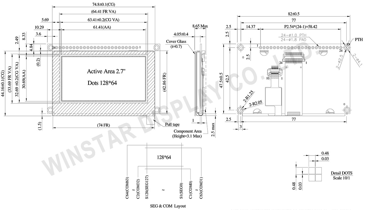
WEP012864Q-CTP 是一款含電容式觸控COG繪圖型OLED顯示器,有效區域對角線為2.7吋,解析度128x64 pixels。此OLED模組內建SSD1309 IC 可支援6800/8080 8-bit、I2C、4線SPI等介面。邏輯電壓為3V;驅動方式為1/64 duty;50%顯示畫面耗電為175mA @ 3.0V(典型值)。模組含電容式觸控面板並內建GT911 IC支援I2C介面和1點觸控,表面採用亮面玻璃。此型號OLED模組加上PCB設計可使用導線連接,客戶不需要額外自行開發PCB版,整合了介面設定和VCC電路,使客戶易於使用。模組工作溫度範圍-20℃~+70℃;儲存溫度範圍 -30℃~+80℃,適合用在智能家電、醫療設備、工控設備等等。
Data source ref: WEP012864QWPP3D00000
| 項目 | 尺寸 | 單位 |
|---|---|---|
| 點陣(解析度) | 128 x 64 | - |
| 模組尺寸 | 82.0 × 47.5 × 8.65 Max. | mm |
| 有效區域 | 61.41 × 30.69 | mm |
| 點大小 | 0.45 × 0.45 | mm |
| 點間距 | 0.48 × 0.48 | mm |
| 顯示模式 | 被動矩陣 | |
| 顯示顏色 | 單色 | |
| 驅動方式 | 1/64 Duty | |
| IC | SSD1309 | |
| 介面 | 6800,8080,4-Wire SPI,I2C | |
| 尺寸 | 2.7 吋 | |
| CTP IC | GT911 | |
| 支援手指數 | 1 | |
| CTP 介面 | I2C | |
| 表面 | 亮面 | |
| 參數 | 符號 | 最小值 | 最大值 | 單位 |
|---|---|---|---|---|
| 邏輯電源電壓 | VDD | -0.3 | 4 | V |
| 工作溫度 | TOP | -20 | +70 | °C |
| 儲存溫度 | TSTG | -30 | +80 | °C |
| 項目 | 符號 | 條件 | 最小值 | 典型值 | 最大值 | 單位 |
|---|---|---|---|---|---|---|
| 邏輯電源電壓 | VDD | - | 2.8 | 3.0 | 3.3 | V |
| 輸入高準位 | VIH | - | 0.8×VDD | - | - | V |
| 輸入低準位 | VIL | - | - | - | 0.2×VDD | V |
| 輸出高準位 | VOH | - | 0.9×VDD | - | - | V |
| 輸出低準位 | VOL | - | - | - | 0.1×VDD | V |
| 50%顯示畫面耗電流 | VDD =3V | - | 175 | 350 | mA | |
| 項目 | 符號 | 最小值 | 典型值 | 最大值 | 單位 |
|---|---|---|---|---|---|
| 輸入高準位 | VIH | 0.75xVDD | VDD+0.3 | V | |
| I輸入低準位 | VIL | -0.3 | - | 0.25xVDD | V |
| 輸出高準位 | VOH | 0.85xVDD | - | - | V |
| 輸出低準位 | VOL | - | - | 0.15xVDD | V |
| No. | 符號 | 功能說明 | |||||||||||||||
|---|---|---|---|---|---|---|---|---|---|---|---|---|---|---|---|---|---|
| 1 | VSS | Ground. | |||||||||||||||
| 2 | VDD | Power supply pin for core logic operation | |||||||||||||||
| 3 | NC | No connection | |||||||||||||||
| 4 | D/C# | This pin is Data/Command control pin connecting to the MCU. When the pin is pulled HIGH, the data at D[7:0] will be interpreted as data. When the pin is pulled LOW, the data at D[7:0] will be transferred to a command register. In I2C mode, this pin acts as SA0 for slave address selection. |
|||||||||||||||
| 5 | R/W# (WR#) |
This pin is read / write control input pin connecting to the MCU interface. When 6800 interface mode is selected, this pin will be used as Read/Write (R/W#) selection input. Read mode will be carried out when this pin is pulled HIGH and write mode when LOW. When 8080 interface mode is selected, this pin will be the Write (WR#) input. Data write operation is initiated when this pin is pulled LOW and the chip is selected. When serial or I2C interface is selected, this pin must be connected to VSS. |
|||||||||||||||
| 6 | E(/RD#) | This pin is MCU interface input. When 6800 interface mode is selected, this pin will be used as the Enable (E) signal. Read/write operation is initiated when this pin is pulled HIGH and the chip is selected. When 8080 interface mode is selected, this pin receives the Read (RD#) signal. Read operation is initiated when this pin is pulled LOW and the chip is selected. When serial or I2C interface is selected, this pin must be connected to VSS. |
|||||||||||||||
| 7-14 | D0~D7 | These pins are bi-directional data bus connecting to the MCU data bus. Unused pins are recommended to tie LOW. When serial interface mode is selected, D0 will be the serial clock input: SCLK; D1 will be the serial data input: SDIN and D2 should be kept NC. When I2C mode is selected, D2, D1 should be tied together and serve as SDAout, SDAin in application and D0 is the serial clock input, SCL. |
|||||||||||||||
| 15 | NC | No connection | |||||||||||||||
| 16 | RES# | This pin is reset signal input. When the pin is pulled LOW, initialization of the chip is executed. Keep this pin pull HIGH during normal operation. |
|||||||||||||||
| 17 | CS# | This pin is the chip select input connecting to the MCU. The chip is enabled for MCU communication only when CS# is pulled LOW (active LOW). |
|||||||||||||||
| 18 | NC | No connection | |||||||||||||||
| 19 | BS2 | MCU bus interface selection pins. Select appropriate logic setting as described in the following table. BS2 and BS1 are pin select
(1) 0 is connected to VSS (2) 1 is connected to VDD |
|||||||||||||||
| 20 | BS1 | ||||||||||||||||
| 21 | TP_SCK | I2C clock signal | |||||||||||||||
| 22 | TP_SDA | I2C data signal | |||||||||||||||
| 23 | TP_INT | External interrupt signal, active low | |||||||||||||||
| 24 | TP_RST | External reset signal, active low |

通過點擊「允許所有 Cookie」,代表您同意在您的設備上存儲 Cookie 以增強網站瀏覽體驗、分析網站使用情況並協助我們的行銷和網站效能優化工作。您可以在我們的隱私權政策中找到有關於此的更多資訊。