
 配備鐵框 - WEF012864U")

我們重視您的隱私
通過點擊「允許所有 Cookie」,代表您同意在您的設備上存儲 Cookie 以增強網站瀏覽體驗、分析網站使用情況並協助我們的行銷和網站效能優化工作。您可以在我們的隱私權政策中找到有關於此的更多資訊。


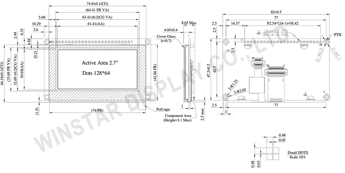
WEP012864U-CTP 是一款 COG 繪圖型 OLED 顯示器模組,採用電容式觸控面板,解析度為 128x64 點,有效區域為 2.7 吋 (61.41 × 30.69 mm) 。 此模組配備SSD1357 IC,支援6800/8080 8位元和4線SPI,以及I2C介面。 此顯示器支援4位元灰度,邏輯電壓為3V,佔空比為1/64。 電容式觸控螢幕內建IC GT911,支援I2C接口與1點觸控功能。
WEP012864U-CTP OLED 系列配有金屬框架和 PCB 板,可透過電線輕鬆連接到應用程式。 客戶無需自行開發額外的PCB板,整合了介面設定和VCC電路,簡化了使用者體驗。 PCB上設計有四個螺孔,方便模組安裝在應用產品上。
此 OLED 模組擁有 10,000:1 的高對比度,可呈現更鮮豔、更深的黑色以及更明亮的白色。 這可以提高影像品質、更清晰的細節並提高可讀性。 模組的工作溫度範圍為-20℃至70℃,儲存溫度範圍為-30℃至80℃。WEP012864U採用CTP觸控螢幕,非常適合智慧家庭應用、高科技設備、儀表設備、工業控制系統、醫療儀器等。
Data source ref: WEP012864UWPP3D00000
| 項目 | 尺寸 | 單位 |
|---|---|---|
| 點陣(解析度) | 128 x 64 | - |
| 模組尺寸 | 82.0 × 47.5 × 8.65 Max. | mm |
| 有效區域 | 61.41 × 30.69 | mm |
| 點大小 | 0.45 × 0.45 | mm |
| 點間距 | 0.48 × 0.48 | mm |
| 顯示模式 | 被動矩陣 | |
| 顯示顏色 | 單色 | |
| 驅動方式 | 1/64 Duty | |
| 灰階 | 4 bits | |
| IC | SSD1357 | |
| 介面 | 8-bits 6800 和 8080 並列, 4線 SPI, I2C | |
| 尺寸 | 2.7 吋 | |
| CTP IC | GT911 |
| 支援手指數 | 1 |
| CTP 介面 | I2C |
| 表面 | 亮面 |
| 參數 | 符號 | 最小值 | 最大值 | 單位 |
|---|---|---|---|---|
| 邏輯電源電壓 | VDD | -0.3 | 4.0 | V |
| 工作溫度 | TOP | -20 | +70 | °C |
| 儲存溫度 | TSTG | -30 | +80 | °C |
| 項目 | 符號 | 條件 | 最小值 | 典型值 | 最大值 | 單位 |
|---|---|---|---|---|---|---|
| 邏輯電源電壓 | VDD | - | 2.8 | 3.0 | 3.3 | V |
| 輸入高準位 | VIH | - | 0.8×VDD | - | - | V |
| 輸入低準位 | VIL | - | - | - | 0.2×VDD | V |
| 輸出高準位 | VOH | - | 0.9×VDD | - | - | V |
| 輸出低準位 | VOL | - | - | - | 0.1×VDD | V |
| 50%顯示畫面耗電流 | IDD | VDD =3V | - | 160 | 240 | mA |
| No. | 符號 | 功能說明 | |||||||||||||||
|---|---|---|---|---|---|---|---|---|---|---|---|---|---|---|---|---|---|
| 1 | VSS | This is a ground pin. | |||||||||||||||
| 2 | VDD | Power supply pin for core logic operation | |||||||||||||||
| 3 | NC | Reserved Pin The N.C. pin between function pins is reserved for compatible and flexible design. |
|||||||||||||||
| 4 | D/C# | This pin is Data/Command control pin connecting to the MCU. When the pin is pulled HIGH, the data at D[7:0] will be interpreted as data. When the pin is pulled LOW, the data at D[7:0] will be transferred to a command register. In I2C mode, this pin acts as SA0 for slave address selection. When 3-wire serial interface is selected, this pin must be connected to VSS. |
|||||||||||||||
| 5 | R/W# (WR#) |
This pin is read / write control input pin connecting to the MCU interface. When 6800 interface mode is selected, this pin will be used as Read/Write (R/W#) selection input. Read mode will be carried out when this pin is pulled HIGH and write mode when LOW. When 8080 interface mode is selected, this pin will be the Write (WR#) input. Data write operation is initiated when this pin is pulled LOW and the chip is selected. When serial or I2C interface is selected, this pin must be connected to VSS. |
|||||||||||||||
| 6 | E/RD# | This pin is MCU interface input. When 6800 interface mode is selected, this pin will be used as the Enable (E) signal. Read/write operation is initiated when this pin is pulled HIGH and the chip is selected. When 8080 interface mode is selected, this pin receives the Read (RD#) signal. Read operation is initiated when this pin is pulled LOW and the chip is selected. When serial or I2C interface is selected, this pin must be connected to VSS. |
|||||||||||||||
| 7 | DB0 | These pins are bi-directional data bus connecting to the MCU data bus. Unused pins are recommended to tie LOW. When serial interface mode is selected, D0 will be the serial clock input: SCLK; D1 will be the serial data input: SDIN. When I2C mode is selected, D2, D1 should be tied together and serve as SDAout, SDAin in application and D0 is the serial clock input, SCL. |
|||||||||||||||
| 8 | DB1 | ||||||||||||||||
| 9 | DB2 | ||||||||||||||||
| 10 | DB3 | ||||||||||||||||
| 11 | DB4 | ||||||||||||||||
| 12 | DB5 | ||||||||||||||||
| 13 | DB6 | ||||||||||||||||
| 14 | DB7 | ||||||||||||||||
| 15 | NC | No connection | |||||||||||||||
| 16 | RES# | This pin is reset signal input. When the pin is pulled LOW, initialization of the chip is executed. Keep this pin pull HIGH during normal operation. |
|||||||||||||||
| 17 | CS# | Chip Select This pin is the chip select input. The chip is enabled for MCU communication only when CS# is pulled low. |
|||||||||||||||
| 18 | NC | No connection | |||||||||||||||
| 19 | BS2 | Communicating Protocol Select. These pins are MCU interface selection input. See the following table:
|
|||||||||||||||
| 20 | BS1 | ||||||||||||||||
| 21 | TP_SCK | I2C clock signal | |||||||||||||||
| 22 | TP_SDA | I2C data signal | |||||||||||||||
| 23 | TP_INT | Interrupt signal, active low, asserted to request Host start a new transaction |
|||||||||||||||
| 24 | TP_RST | External reset signal, active low |

通過點擊「允許所有 Cookie」,代表您同意在您的設備上存儲 Cookie 以增強網站瀏覽體驗、分析網站使用情況並協助我們的行銷和網站效能優化工作。您可以在我們的隱私權政策中找到有關於此的更多資訊。