Accueil Produits Module OLED Écran tactile OLED WEP012864U-CTP

2.7", 128x64 Modules afficheurs COG OLED Frame +PCB

N° de modèle WEP012864U-CTP

►Type: Graphique
►Structure: COG + cadre + PCB
►Dimension: 2.7 pouces
►Matrice de points 128 x 64
►IC:SSD1357
►Alimentation 3V
►1/64 duty
►Interface: 6800, 8080, SPI, I2C
►Dalle tactile: Avec dalle tactile capacitive (CTP)
►Points tactiles: 1 Doigt
►Couleur d'affichage: Blanc / Jaune
►Support d’échelle grise

Description

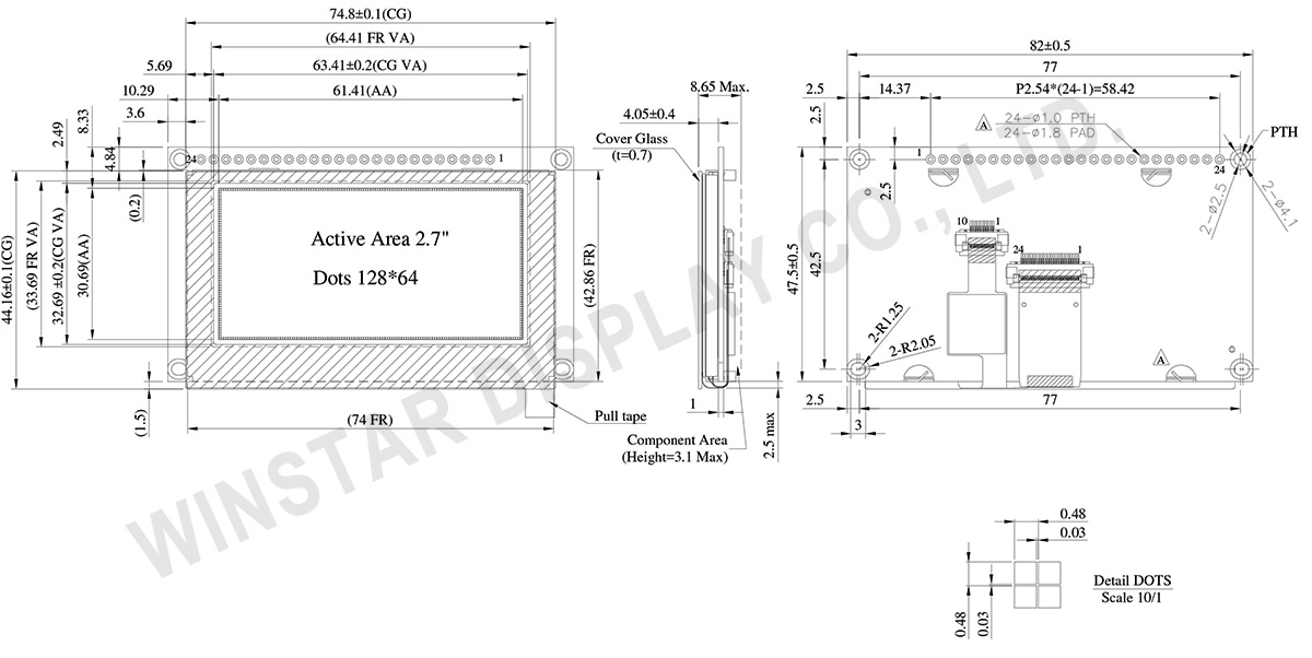
WEP012864U-CTP est un écran OLED graphique COG avec un panneau tactile capacitif, d'une résolution de 128x64 pixels et d'une zone active de 2,7 pouces (61,41 x 30,69 mm). Le circuit intégré SSD1357 de ce module prend en charge les interfaces 6800/8080 8 bits et SPI à 4 fils, ainsi que l'interface I2C. L'écran prend en charge 4 bits de niveaux de gris, avec une tension logique de 3V et un cycle de fonctionnement de 1/64. Le panneau tactile capacitif intègre le circuit intégré GT911, prenant en charge une interface I2C avec une capacité de toucher à un point.

La série OLED WEP012864U-CTP est dotée d'un cadre métallique et d'une carte de circuit imprimé qui se connecte facilement à l'application via des fils. Les clients n'ont pas besoin de développer eux-mêmes des cartes de circuit imprimé supplémentaires. Il intègre des réglages d'interface et des circuits VCC, ce qui facilite l'utilisation pour les clients. Quatre trous filetés sont conçus sur la carte de circuit imprimé pour faciliter l'installation du module sur le produit d'application.

Ce module OLED offre un taux de contraste élevé de 10 000:1, ce qui permet des noirs plus vibrants et plus profonds, ainsi que des blancs plus lumineux. Cela se traduit par une qualité d'image améliorée, des détails plus nets et une lisibilité améliorée. Le module peut fonctionner dans une plage de températures de -20°C à 70°C, avec des températures de stockage allant de -30°C à 80°C.

Le WEP012864U avec panneau tactile CTP convient très bien aux applications de maison intelligente, aux équipements haute technologie, aux équipements de mesure, aux systèmes de contrôle industriel, aux instruments médicaux, etc.

DESSIN

WEP012864U-CTP
 

Data source ref: WEP012864UWPP3D00000

SPÉCIFICATIONS

Fonction PIN sur l'interface

No. Symbol Fonction
1 VSS This is a ground pin.
2 VDD Power supply pin for core logic operation
3 NC Reserved Pin
The N.C. pin between function pins is reserved for compatible and flexible design.
4 D/C# This pin is Data/Command control pin connecting to the MCU.
When the pin is pulled HIGH, the data at D[7:0] will be interpreted as data.
When the pin is pulled LOW, the data at D[7:0] will be transferred to a command register.
In I2C mode, this pin acts as SA0 for slave address selection.
When 3-wire serial interface is selected, this pin must be connected to VSS.
5 R/W#
(WR#)
This pin is read / write control input pin connecting to the MCU interface.
When 6800 interface mode is selected, this pin will be used as Read/Write (R/W#) selection input. Read mode will be carried out when this pin is pulled HIGH and write mode when LOW.
When 8080 interface mode is selected, this pin will be the Write (WR#) input. Data write operation is initiated when this pin is pulled LOW and the chip is selected.
When serial or I2C interface is selected, this pin must be connected to VSS.
6 E/RD# This pin is MCU interface input.
When 6800 interface mode is selected, this pin will be used as the Enable (E) signal.
Read/write operation is initiated when this pin is pulled HIGH and the chip is selected.
When 8080 interface mode is selected, this pin receives the Read (RD#) signal. Read operation is initiated when this pin is pulled LOW and the chip is selected.
When serial or I2C interface is selected, this pin must be connected to VSS.
7 DB0 These pins are bi-directional data bus connecting to the MCU data bus.
Unused pins are recommended to tie LOW.
When serial interface mode is selected, D0 will be the serial clock input: SCLK; D1 will be the serial data input: SDIN.
When I2C mode is selected, D2, D1 should be tied together and serve as SDAout, SDAin in application and D0 is the serial clock input, SCL.
8 DB1
9 DB2
10 DB3
11 DB4
12 DB5
13 DB6
14 DB7
15 NC No connection
16 RES# This pin is reset signal input.
When the pin is pulled LOW, initialization of the chip is executed.
Keep this pin pull HIGH during normal operation.
17 CS# Chip Select
This pin is the chip select input. The chip is enabled for MCU communication only when CS# is pulled low.
18 NC No connection
19 BS2 Communicating Protocol Select.
These pins are MCU interface selection input. See the following table:
  BS1 BS2
I2C 1 0
4-wire Serial 0 0
8-bit 8080 Parallel 1 1
8-bit 6800 Parallel 0 1
20 BS1
21 TP_SCK I2C clock signal
22 TP_SDA I2C data signal
23 TP_INT Interrupt signal, active low, asserted to request
Host start a new transaction
24 TP_RST External reset signal, active low

Données mécaniques

Article Dimensions Unité
Matrice de points 128 × 64
Dimensions du module 82.0 × 47.5 × 8.65 Max. mm
Zone active 61.41 × 30.69 mm
Pixel Size 0.45 × 0.45 mm
Pixel Pitch 0.48 × 0.48 mm
Mode d'affichage Matrice passive
Couleur d'affichage Monochrome
Drive Duty 1/64 Duty
Gray Scale 4 bits
IC SSD1357
Interface 8-bits 6800 and 8080 parallel, 4-line SPI, I2C
Diagonale 2.7 pouces
 
CTP IC GT911
Points tactiles 1
CTP Interface I2C
Surface Reflets

Valeurs nominales maximales absolues

Parameter Symbole Min Max Unité
Supply Voltage for Logic VDD -0.3 4.0 V
Température de fonctionnement TOP -20 +70 °C
Température de stockage TSTG -30 +80 °C

Caractéristiques électroniques

DC Caractéristiques électroniques

Article Symbole État Min Typ Max Unité
Supply Voltage for Logic VDD 2.8 3.0 3.3 V
High Level Input VIH 0.8×VDD V
Low Level Input VIL 0.2×VDD V
High Level Output VOH 0.9×VDD V
Low Level Output VOL 0.1×VDD V
50% Check Board operating Current IDD VDD =3V 160 240 mA

Search keyword: 128x64 oled, oled 128x64, 2.7 oled, 2.7 pouces oled, oled 2.7"
go top
close