2,7", 128x64 kapazitives Touch-Panel OLED-Anzeigemodule + Frame +PCB
Modellnummer WEP012864U-CTP
►Typ: Grafik
►Bauweise: COG + Frame + PCB
►Größe: 2,7 Zoll
►128 x 64 Punktmatrix
►IC:SSD1357
►3-V-Stromversorgung
►1/64 duty
►Schnittstelle: 6800, 8080, SPI, I2C
►Touch Panel: kapazitives Touch-Panel (CTP)
►Berührungspunkte : 1 Finger
►die Farbe des Displays: Weiß / Gelb
►Unterstützt Grauskala
Beschreibung
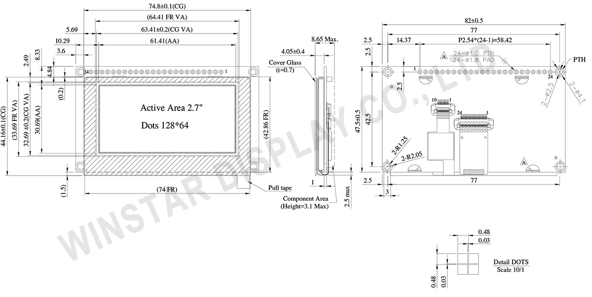
WEP012864U-CTP ist ein COG-Grafik-OLED-Display mit kapazitivem Touchscreen, einer Auflösung von 128x64 Pixeln und einer aktiven Fläche von 2,7 Zoll (61,41 x 30,69 mm). Der integrierte SSD1357-IC unterstützt die 6800/8080 8-Bit- und 4-Draht-SPI- sowie I2C-Schnittstellen. Der Bildschirm unterstützt 4-Bit-Graustufen, mit einer Logikspannung von 3V und einer Arbeitszyklus von 1/64. Das kapazitive Touchpanel enthält den integrierten IC GT911, der eine I2C-Schnittstelle mit 1-Punkt-Touch unterstützt.
Die OLED-Serie WEP012864U-CTP verfügt über einen Metallrahmen und eine Leiterplatte, die sich über Drähte leicht mit der Anwendung verbinden lässt. Kunden müssen keine zusätzlichen Leiterplatten selbst entwickeln. Die integrierten Schnittstelleneinstellungen und VCC-Schaltungen erleichtern die Verwendung des Moduls. Auf der Leiterplatte befinden sich vier Schraublöcher, um das Modul einfach auf dem Anwendungsprodukt zu installieren.
Dieses OLED-Modul bietet ein hohes Kontrastverhältnis von 10.000:1, was zu lebendigeren und tieferen Schwarztönen sowie helleren Weißtönen führt. Dies führt zu einer verbesserten Bildqualität, schärferen Details und verbesserter Lesbarkeit. Das Modul kann in Temperaturen von -20°C bis 70°C betrieben werden, wobei die Lagertemperaturen von -30°C bis 80°C reichen.
WEP012864U mit CTP-Touchpanel eignet sich sehr gut für Smart-Home-Anwendungen, High-Tech-Geräte, Messgeräte, industrielle Steuerungssysteme, medizinische Instrumente usw.
Zeichnung
Data source ref: WEP012864UWPP3D00000
Technische Daten
Schnittstelle Pin-Funktion
No. | Symbol | Beschreibung | |||||||||||||||
---|---|---|---|---|---|---|---|---|---|---|---|---|---|---|---|---|---|
1 | VSS | This is a ground pin. | |||||||||||||||
2 | VDD | Power supply pin for core logic operation | |||||||||||||||
3 | NC | Reserved Pin The N.C. pin between function pins is reserved for compatible and flexible design. |
|||||||||||||||
4 | D/C# | This pin is Data/Command control pin connecting to the MCU. When the pin is pulled HIGH, the data at D[7:0] will be interpreted as data. When the pin is pulled LOW, the data at D[7:0] will be transferred to a command register. In I2C mode, this pin acts as SA0 for slave address selection. When 3-wire serial interface is selected, this pin must be connected to VSS. |
|||||||||||||||
5 | R/W# (WR#) |
This pin is read / write control input pin connecting to the MCU interface. When 6800 interface mode is selected, this pin will be used as Read/Write (R/W#) selection input. Read mode will be carried out when this pin is pulled HIGH and write mode when LOW. When 8080 interface mode is selected, this pin will be the Write (WR#) input. Data write operation is initiated when this pin is pulled LOW and the chip is selected. When serial or I2C interface is selected, this pin must be connected to VSS. |
|||||||||||||||
6 | E/RD# | This pin is MCU interface input. When 6800 interface mode is selected, this pin will be used as the Enable (E) signal. Read/write operation is initiated when this pin is pulled HIGH and the chip is selected. When 8080 interface mode is selected, this pin receives the Read (RD#) signal. Read operation is initiated when this pin is pulled LOW and the chip is selected. When serial or I2C interface is selected, this pin must be connected to VSS. |
|||||||||||||||
7 | DB0 | These pins are bi-directional data bus connecting to the MCU data bus. Unused pins are recommended to tie LOW. When serial interface mode is selected, D0 will be the serial clock input: SCLK; D1 will be the serial data input: SDIN. When I2C mode is selected, D2, D1 should be tied together and serve as SDAout, SDAin in application and D0 is the serial clock input, SCL. |
|||||||||||||||
8 | DB1 | ||||||||||||||||
9 | DB2 | ||||||||||||||||
10 | DB3 | ||||||||||||||||
11 | DB4 | ||||||||||||||||
12 | DB5 | ||||||||||||||||
13 | DB6 | ||||||||||||||||
14 | DB7 | ||||||||||||||||
15 | NC | No connection | |||||||||||||||
16 | RES# | This pin is reset signal input. When the pin is pulled LOW, initialization of the chip is executed. Keep this pin pull HIGH during normal operation. |
|||||||||||||||
17 | CS# | Chip Select This pin is the chip select input. The chip is enabled for MCU communication only when CS# is pulled low. |
|||||||||||||||
18 | NC | No connection | |||||||||||||||
19 | BS2 | Communicating Protocol Select. These pins are MCU interface selection input. See the following table:
|
|||||||||||||||
20 | BS1 | ||||||||||||||||
21 | TP_SCK | I2C clock signal | |||||||||||||||
22 | TP_SDA | I2C data signal | |||||||||||||||
23 | TP_INT | Interrupt signal, active low, asserted to request Host start a new transaction |
|||||||||||||||
24 | TP_RST | External reset signal, active low |
mechanische Daten
Artikel | Ausmaß | Einheit |
---|---|---|
Punktmatrix | 128 × 64 | - |
Abmaße der modul | 82,0 × 47,5 × 8,65 Max. | mm |
Aktiver Bereich | 61,41 × 30,69 | mm |
Punktgröße | 0,45 × 0,45 | mm |
Punktabstand | 0,48 × 0,48 | mm |
Display Mode | Passive Matrix | |
Display Color | Monochrome | |
Drive Duty | 1/64 Duty | |
Grauskala | 4 bits | |
IC | SSD1357 | |
Schnittstelle | 8-bits 6800 and 8080 parallel, 4-line SPI, I2C | |
Größe (Diagonale) | 2,7 Zoll |
CTP IC | GT911 |
Berührungspunkte | 1 |
CTP Schnittstelle | I2C |
Oberfläche | Glanz |
Absolute Grenzwerte
Parameter | Symbol | Mindestwert | Maximalwert | Einheit |
---|---|---|---|---|
Supply Voltage for Logic | VDD | -0,3 | 4,0 | V |
Betriebstemperatur | TOP | -20 | +70 | °C |
Lagertemperatur | TSTG | -30 | +80 | °C |
elektronische Eingenschaften
DC elektronische Eingenschaften
Artikel | Symbol | Bedingung | Mindestwert | typischer Wert | Maximalwert | Einheit |
---|---|---|---|---|---|---|
Supply Voltage for Logic | VDD | - | 2,8 | 3,0 | 3,3 | V |
High Level Input | VIH | - | 0,8×VDD | - | - | V |
Low Level Input | VIL | - | - | - | 0,2×VDD | V |
High Level Output | VOH | - | 0,9×VDD | - | - | V |
Low Level Output | VOL | - | - | - | 0,1×VDD | V |
50% Check Board operating Current | IDD | VDD =3V | - | 160 | 240 | mA |