- WEO012864U")
 - WEF012864U")


私たちはあなたのプライバシーを大切にします
「すべてのクッキーを許可」をクリックすると、サイトのナビゲーションを向上させ、サイト使用状況を分析し、マーケティングおよびパフォーマンスの取り組みを支援するために、クッキーをデバイスに保存することに同意したことになります。この件に関する詳細情報は、ポリシーをご覧ください。プライバシーポリシー


型番 WEP012864U-CTP
►タイプ: グラフィック有機ELディスプレイ
►結構: COG + 鉄フレーム + PCB
►サイズ: 2.7インチ
►128 x 64 ドットマトリックス
►IC:SSD1357
►3V電源電圧
►1/64 duty
►インターフェース: 6800, 8080, SPI, I2C
►静電容量式タッチパネル(CTP)
►検出ポイント: 1
►発光色: 白色 / 黄色
►グレースケール機能をサポートする
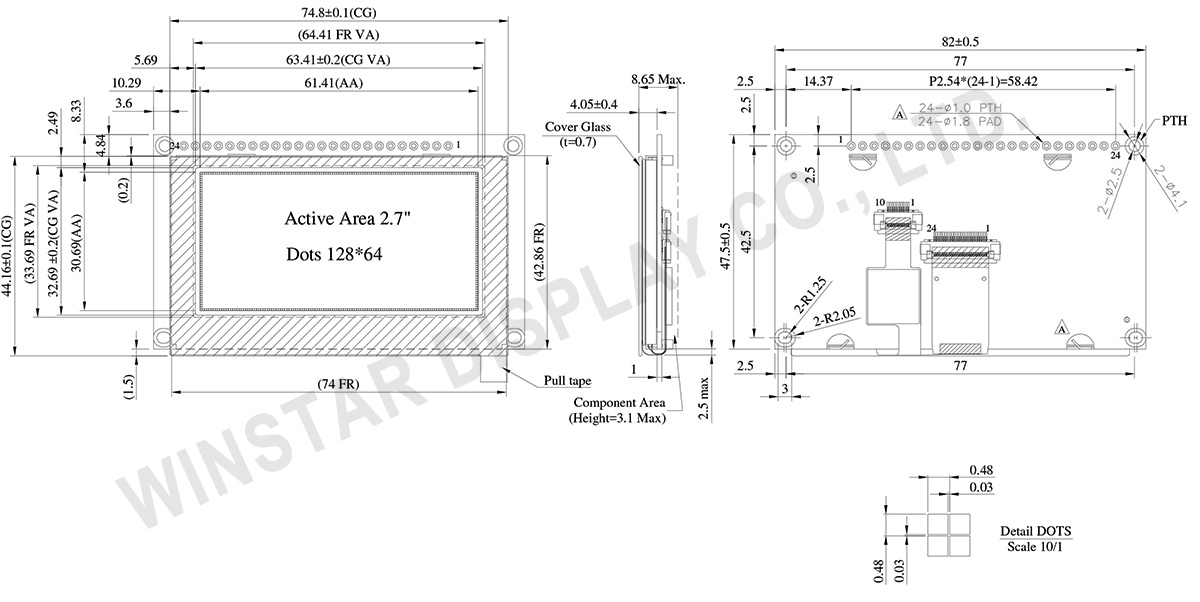
WEP012864U-CTPは、解像度128x64ドット、有効表示領域2.7インチ(61.41×30.69mm)のCOGグラフィックOLEDディスプレイで、静電容量タッチパネルが搭載されています。モジュールにはSSD1357 ICが搭載されており、6800/8080 8ビットおよび4線SPI、I2Cインターフェースに対応しています。ディスプレイは4ビットの階調をサポートし、ロジック電圧は3Vで、デューティサイクルは1/64です。静電容量タッチパネルには、内蔵IC GT911が搭載されており、1ポイントタッチのI2Cインターフェースに対応しています。
WEP012864U-CTP OLEDシリーズには、ワイヤーを介してアプリケーションに簡単に接続できる金属フレームとPCBボードが付属しています。顧客は追加のPCBボードを自ら開発する必要はありません。インターフェース設定とVCC回路が統合されており、顧客が使用する際に便利です。PCBには4つのねじ穴が設計されており、アプリケーション製品にモジュールを簡単に取り付けることができます。
このOLEDモジュールは、10,000:1という高いコントラスト比を誇り、より鮮明で深い黒と明るい白を実現します。これにより、画像の品質が向上し、より鮮明なディテールと改善された読みやすさが得られます。モジュールは-20℃から70℃の温度範囲で動作し、-30℃から80℃の温度範囲で保管できます。
CTPタッチパネルを搭載したWEP012864Uは、スマートホームアプリケーション、ハイテク機器、メーター機器、産業制御システム、医療機器などに非常に適しています。
Data source ref: WEP012864UWPP3D00000
| 項目 | 仕様 | 単位 |
|---|---|---|
| ドットマトリックス(解像度) | 128 x 64 | - |
| モジュールサイズ | 82.0 × 47.5 × 8.65 Max. | mm |
| 有効エリア | 61.41 × 30.69 | mm |
| ドットサイズ | 0.45 × 0.45 | mm |
| ドットピッチ | 0.48 × 0.48 | mm |
| 表示モード | パッシブマトリクス | |
| 発光色 | モノクロ | |
| 駆動方法 | 1/64 Duty | |
| グレースケール | 4 bits | |
| IC | SSD1357 | |
| インターフェイス | 8-bits 6800 and 8080 parallel, 4-line SPI, I2C | |
| 表示サイズ | 2.7インチ | |
| CTP IC | GT911 |
| 検出ポイント | 1 |
| CTP インターフェイス | I2C |
| 表面処理 | グレア |
| パラメーター | 記号 | 最小値 | 最大値 | 単位 |
|---|---|---|---|---|
| ロジック電源電圧 | VDD | -0.3 | 4.0 | V |
| 操作温度 | TOP | -20 | +70 | °C |
| 保存温度 | TSTG | -30 | +80 | °C |
| 項目 | 記号 | 条件 | 最小値 | 典型値 | 最大値 | 単位 |
|---|---|---|---|---|---|---|
| ロジック電源電圧 | VDD | - | 2.8 | 3.0 | 3.3 | V |
| 高レベル入力 | VIH | - | 0.8×VDD | - | - | V |
| 低レベル入力 | VIL | - | - | - | 0.2×VDD | V |
| 高レベル出力 | VOH | - | 0.9×VDD | - | - | V |
| 低レベル出力 | VOL | - | - | - | 0.1×VDD | V |
| 50% Check Board operating Current | IDD | VDD =3V | - | 160 | 240 | mA |
| No. | 記号 | 説明 | |||||||||||||||
|---|---|---|---|---|---|---|---|---|---|---|---|---|---|---|---|---|---|
| 1 | VSS | This is a ground pin. | |||||||||||||||
| 2 | VDD | Power supply pin for core logic operation | |||||||||||||||
| 3 | NC | Reserved Pin The N.C. pin between function pins is reserved for compatible and flexible design. |
|||||||||||||||
| 4 | D/C# | This pin is Data/Command control pin connecting to the MCU. When the pin is pulled HIGH, the data at D[7:0] will be interpreted as data. When the pin is pulled LOW, the data at D[7:0] will be transferred to a command register. In I2C mode, this pin acts as SA0 for slave address selection. When 3-wire serial interface is selected, this pin must be connected to VSS. |
|||||||||||||||
| 5 | R/W# (WR#) |
This pin is read / write control input pin connecting to the MCU interface. When 6800 interface mode is selected, this pin will be used as Read/Write (R/W#) selection input. Read mode will be carried out when this pin is pulled HIGH and write mode when LOW. When 8080 interface mode is selected, this pin will be the Write (WR#) input. Data write operation is initiated when this pin is pulled LOW and the chip is selected. When serial or I2C interface is selected, this pin must be connected to VSS. |
|||||||||||||||
| 6 | E/RD# | This pin is MCU interface input. When 6800 interface mode is selected, this pin will be used as the Enable (E) signal. Read/write operation is initiated when this pin is pulled HIGH and the chip is selected. When 8080 interface mode is selected, this pin receives the Read (RD#) signal. Read operation is initiated when this pin is pulled LOW and the chip is selected. When serial or I2C interface is selected, this pin must be connected to VSS. |
|||||||||||||||
| 7 | DB0 | These pins are bi-directional data bus connecting to the MCU data bus. Unused pins are recommended to tie LOW. When serial interface mode is selected, D0 will be the serial clock input: SCLK; D1 will be the serial data input: SDIN. When I2C mode is selected, D2, D1 should be tied together and serve as SDAout, SDAin in application and D0 is the serial clock input, SCL. |
|||||||||||||||
| 8 | DB1 | ||||||||||||||||
| 9 | DB2 | ||||||||||||||||
| 10 | DB3 | ||||||||||||||||
| 11 | DB4 | ||||||||||||||||
| 12 | DB5 | ||||||||||||||||
| 13 | DB6 | ||||||||||||||||
| 14 | DB7 | ||||||||||||||||
| 15 | NC | No connection | |||||||||||||||
| 16 | RES# | This pin is reset signal input. When the pin is pulled LOW, initialization of the chip is executed. Keep this pin pull HIGH during normal operation. |
|||||||||||||||
| 17 | CS# | Chip Select This pin is the chip select input. The chip is enabled for MCU communication only when CS# is pulled low. |
|||||||||||||||
| 18 | NC | No connection | |||||||||||||||
| 19 | BS2 | Communicating Protocol Select. These pins are MCU interface selection input. See the following table:
|
|||||||||||||||
| 20 | BS1 | ||||||||||||||||
| 21 | TP_SCK | I2C clock signal | |||||||||||||||
| 22 | TP_SDA | I2C data signal | |||||||||||||||
| 23 | TP_INT | Interrupt signal, active low, asserted to request Host start a new transaction |
|||||||||||||||
| 24 | TP_RST | External reset signal, active low |

「すべてのクッキーを許可」をクリックすると、サイトのナビゲーションを向上させ、サイト使用状況を分析し、マーケティングおよびパフォーマンスの取り組みを支援するために、クッキーをデバイスに保存することに同意したことになります。この件に関する詳細情報は、ポリシーをご覧ください。プライバシーポリシー