2.7" 128x64 дюймовый COG OLED с емкостной сенсорной тач панелью + Frame +PCB
Numer modelu WEP012864U-CTP
►Typ: graficzny
►Struktura: COG + ramki + PCB
►Rozmiar: 2.7"
►128 x 64 matryca punktowa
►IC:SSD1357
►zasilanie 3V
►wypełnienie 1/64
►Interfejs: 6800, 8080, SPI, I2C
►Panel dotykowy: pojemnościowy panel dotykowy (CTP)
►Punkty dotyku: 1 Palec
►Kolor wyświetlacza: biały / żółto
►Obsługiwana skala szarości
Opis
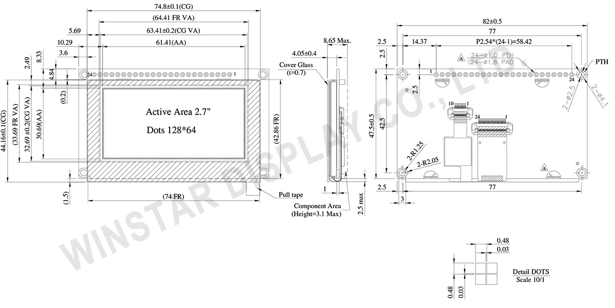
WEP012864U-CTP to graficzny moduł OLED COG z pojemnościowym panelem dotykowym, o rozdzielczości 128x64 punktów i aktywnej powierzchni 2,7 cala (61,41 x 30,69 mm). Zintegrowany układ SSD1357 obsługuje interfejsy 6800/8080 8-bitowy oraz 4-przewodowy SPI, a także I2C. Wyświetlacz obsługuje 4-bitową skalę szarości, z napięciem logicznym 3V i cyklem pracy 1/64. Panel dotykowy pojemnościowy zawiera wbudowany układ GT911, obsługujący interfejs I2C z możliwością jednego punktu dotyku.
Seria OLED WEP012864U-CTP posiada ramę metalową oraz płytę PCB, która łatwo łączy się z aplikacją za pomocą przewodów. Klienci nie muszą samodzielnie rozwijać dodatkowych płyt PCB. Zintegrowane ustawienia interfejsu i obwody VCC ułatwiają korzystanie z modułu. Na PCB zaprojektowano cztery otwory na śruby, ułatwiające montaż modułu na produkcie aplikacyjnym.
Ten moduł OLED posiada wysoki stosunek kontrastu 10 000:1, co pozwala na bardziej wyraziste i głębokie czernie oraz jaśniejsze biel. Skutkuje to poprawą jakości obrazu, wyraźniejszymi detalami i lepszą czytelnością. Moduł może działać w temperaturach od -20°C do 70°C, a jego temperatury przechowywania wahają się od -30°C do 80°C.
WEP012864U z panelem dotykowym CTP jest bardzo odpowiedni do zastosowań w inteligentnych domach, urządzeniach nowej technologii, urządzeniach pomiarowych, systemach kontroli przemysłowej, przyrządach medycznych itp.
Rysunek
Data source ref: WEP012864UWPP3D00000
Specyfikacja
Funkcja pinów interfejsu
No. | Symbol | Funkcja | |||||||||||||||
---|---|---|---|---|---|---|---|---|---|---|---|---|---|---|---|---|---|
1 | VSS | This is a ground pin. | |||||||||||||||
2 | VDD | Power supply pin for core logic operation | |||||||||||||||
3 | NC | Reserved Pin The N.C. pin between function pins is reserved for compatible and flexible design. |
|||||||||||||||
4 | D/C# | This pin is Data/Command control pin connecting to the MCU. When the pin is pulled HIGH, the data at D[7:0] will be interpreted as data. When the pin is pulled LOW, the data at D[7:0] will be transferred to a command register. In I2C mode, this pin acts as SA0 for slave address selection. When 3-wire serial interface is selected, this pin must be connected to VSS. |
|||||||||||||||
5 | R/W# (WR#) |
This pin is read / write control input pin connecting to the MCU interface. When 6800 interface mode is selected, this pin will be used as Read/Write (R/W#) selection input. Read mode will be carried out when this pin is pulled HIGH and write mode when LOW. When 8080 interface mode is selected, this pin will be the Write (WR#) input. Data write operation is initiated when this pin is pulled LOW and the chip is selected. When serial or I2C interface is selected, this pin must be connected to VSS. |
|||||||||||||||
6 | E/RD# | This pin is MCU interface input. When 6800 interface mode is selected, this pin will be used as the Enable (E) signal. Read/write operation is initiated when this pin is pulled HIGH and the chip is selected. When 8080 interface mode is selected, this pin receives the Read (RD#) signal. Read operation is initiated when this pin is pulled LOW and the chip is selected. When serial or I2C interface is selected, this pin must be connected to VSS. |
|||||||||||||||
7 | DB0 | These pins are bi-directional data bus connecting to the MCU data bus. Unused pins are recommended to tie LOW. When serial interface mode is selected, D0 will be the serial clock input: SCLK; D1 will be the serial data input: SDIN. When I2C mode is selected, D2, D1 should be tied together and serve as SDAout, SDAin in application and D0 is the serial clock input, SCL. |
|||||||||||||||
8 | DB1 | ||||||||||||||||
9 | DB2 | ||||||||||||||||
10 | DB3 | ||||||||||||||||
11 | DB4 | ||||||||||||||||
12 | DB5 | ||||||||||||||||
13 | DB6 | ||||||||||||||||
14 | DB7 | ||||||||||||||||
15 | NC | No connection | |||||||||||||||
16 | RES# | This pin is reset signal input. When the pin is pulled LOW, initialization of the chip is executed. Keep this pin pull HIGH during normal operation. |
|||||||||||||||
17 | CS# | Chip Select This pin is the chip select input. The chip is enabled for MCU communication only when CS# is pulled low. |
|||||||||||||||
18 | NC | No connection | |||||||||||||||
19 | BS2 | Communicating Protocol Select. These pins are MCU interface selection input. See the following table:
|
|||||||||||||||
20 | BS1 | ||||||||||||||||
21 | TP_SCK | I2C clock signal | |||||||||||||||
22 | TP_SDA | I2C data signal | |||||||||||||||
23 | TP_INT | Interrupt signal, active low, asserted to request Host start a new transaction |
|||||||||||||||
24 | TP_RST | External reset signal, active low |
Dane mechaniczne
Rzecz | Wymiar | Jednostka |
---|---|---|
Matryca punktowa | 128 × 64 | - |
Wymiary modułu | 82.0 × 47.5 × 8.65 Max. | mm |
Obszar aktywny | 61.41 × 30.69 | mm |
Wielkość piksela | 0.45 × 0.45 | mm |
Raster pomiędzy pikselami | 0.48 × 0.48 | mm |
Tryb wyświetlania | matryca | |
Kolor wyświetlacza | Monochromatyczny | |
Drive Duty | 1/64 Duty | |
Skala szarości | 4 bits | |
IC | SSD1357 | |
Interfejs | 8-bits 6800 and 8080 parallel, 4-line SPI, I2C | |
Rozmiar (Przekątna) | 2.7 cale |
CTP IC | GT911 |
Punkty dotyku | 1 |
CTP Interfejs | I2C |
Powierzchnia | Glare |
Bezwzględne oceny maksymalne
Parameter | Symbol | Minimalna wartość | Maksymalna wartość | Jednostka |
---|---|---|---|---|
Supply Voltage for Logic | VDD | -0.3 | 4.0 | V |
Temperatura pracy | TOP | -20 | +70 | °C |
Temperatura przechowywania | TSTG | -30 | +80 | °C |
Parametry elektryczne
DC Parametry elektryczne
Rzecz | Symbol | Stan | Minimalna wartość | Typowa wartość | Maksymalna wartość | Jednostka |
---|---|---|---|---|---|---|
Supply Voltage for Logic | VDD | - | 2.8 | 3.0 | 3.3 | V |
High Level Input | VIH | - | 0.8×VDD | - | - | V |
Low Level Input | VIL | - | - | - | 0.2×VDD | V |
High Level Output | VOH | - | 0.9×VDD | - | - | V |
Low Level Output | VOL | - | - | - | 0.1×VDD | V |
50% Check Board operating Current | IDD | VDD =3V | - | 160 | 240 | mA |
Search keyword: 128x64 oled, oled 128x64, 2.7 oled, 2.7 cale oled, oled 2.7"