 - WLEP02566400DGAAASA00")
 - WEO025664D")
私たちはあなたのプライバシーを大切にします
「すべてのクッキーを許可」をクリックすると、サイトのナビゲーションを向上させ、サイト使用状況を分析し、マーケティングおよびパフォーマンスの取り組みを支援するために、クッキーをデバイスに保存することに同意したことになります。この件に関する詳細情報は、ポリシーをご覧ください。プライバシーポリシー

 - WEO025664D-CTP")
 - WEO025664D-CTP")
 - WEO025664D-CTP")
 - WEO025664D-CTP")
 - WEO025664D-CTP")
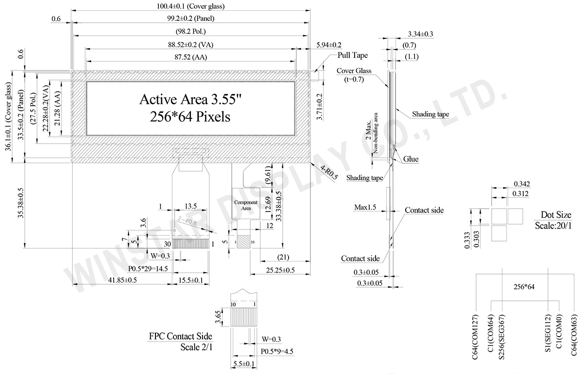
WEO025664D-CTPは、3.55インチのCOG OLEDディスプレイモジュールで、静電容量式タッチパネルを一体化しています。解像度は256×64ドット、SSD1322コントローラICを搭載し、6800/8080 8-bitパラレルおよび3/4線SPIに対応しています。3.3Vロジック電源および16V表示電源、1/64デューティ駆動、4-bitグレースケール表示に対応します。
タッチパネルはFT6336Uコントローラを採用し、I2Cインターフェースおよびシングルタッチ入力に対応しています。COG構造によりコンパクト設計が可能で、省スペース用途に適しています。
動作温度範囲:-20°C~+70°C、保存温度範囲:-30°C~+80°C。スマートホーム、産業機器、医療機器、通信機器などに適しています。
| 項目 | 仕様 | 単位 |
|---|---|---|
| ドットマトリックス | 256 × 64 Dots | - |
| モジュールサイズ | 100.4 × 36.1 × 3.34 | mm |
| アクティブエリア | 87.52 × 21.28 | mm |
| ドットサイズ | 0.312 × 0.303 | mm |
| ドットピッチ | 0.342 × 0.333 | mm |
| 表示モード | パッシブマトリクス | |
| 発光色 | モノクロ | |
| 駆動方法 | 1/64 Duty | |
| グレースケール | 4 bits | |
| OLED IC | SSD1322 | |
| OLED インターフェイス | 6800, 8080, SPI | |
| 表示サイズ(対角線) | 3.55 インチ | |
| CTP IC | FT6336U | |
| 検出ポイント | 1 | |
| CTP インターフェイス | I2C | |
| 表面処理 | グレア | |
| パラメーター | 記号 | 最小値 | 最大値 | 単位 |
|---|---|---|---|---|
| 操作電源電圧 | VCI | -0.3 | 4 | V |
| ロジック電源電圧 | VDD | -0.5 | 2.75 | V |
| I/O Pins 電源電圧 | VDDIO | -0.5 | VCI | V |
| ディスプレイの供給電圧 | VCC | -0.5 | 20 | V |
| 操作温度 | TOP | -20 | +70 | °C |
| 保存温度 | TSTG | -30 | +80 | °C |
| パラメーター | 記号 | 最小値 | 最大値 | 単位 |
|---|---|---|---|---|
| 電源電圧 | VDD | -0.3 | 3.6 | V |
| 項目 | 記号 | 条件 | 最小値 | 典型値 | 最大値 | 単位 |
|---|---|---|---|---|---|---|
| 低圧電源 | VCI | - | 3.1 | 3.3 | 3.5 | V |
| ディスプレイの供給電圧 | VCC | - | 15.5 | 16.0 | 16.5 | V |
| ロジック電源電圧 | VDD | - | 2.4 | - | 2.6 | V |
| I / Oピンの電源 | VDDIO | - | 1.65 | VCI | V | |
| 高レベル入力 | VIH | - | 0.8×VDDIO | - | VDDIO | V |
| 低レベル入力 | VIL | - | 0 | - | 0.2×VDDIO | V |
| 高レベル出力 | VOH | - | 0.9×VDDIO | - | VDDIO | V |
| 低レベル出力 | VOL | - | 0 | - | 0.1×VDDIO | V |
| 50% チェックボード動作電流 | VCC =16V | - | 35 | 55 | mA | |
| 項目 | 記号 | 条件 | 最小値 | 典型値 | 最大値 | 単位 |
|---|---|---|---|---|---|---|
| 電源電圧 | VDD | 2.8 | 3.0 | 3.3 | V | |
| 高レベル入力 | VIH | 0.7×VDD | - | VDD | V | |
| 低レベル入力 | VIL | -0.3 | - | 0.3×VDD | V | |
| 高レベル出力 | VOH | IOH = -0.1mA | 0.7×VDD | - | - | V |
| 低レベル出力 | VOL | IOH = 0.1mA | - | - | 0.3×VDD | V |
| Pin Number | 記号 | I/O | 説明 | ||||||||||
|---|---|---|---|---|---|---|---|---|---|---|---|---|---|
| 1 | ESD_GND | P | Ground | ||||||||||
| 2 | VSS | P | Ground. | ||||||||||
| 3 | VCC | P | Power supply for panel driving voltage. This is also the most positive power voltage supply pin. |
||||||||||
| 4 | VCOMH | P | COM signal deselected voltage level. A capacitor should be connected between this pin and VSS. |
||||||||||
| 5 | VLSS | P | Analog system ground pin. | ||||||||||
| 6~13 | D7~D0 | I/O | Host Data Input/Output Bus These pins are 8-bit bi-directional data bus to be connected to the microprocessor’s data bus. When serial mode is selected, D1 will be the serial data input SDIN and D0 will be the serial clock input SCLK. |
||||||||||
| 14 | E/RD# | I | Read/Write Enable or Read This pin is MCU interface input. When interfacing to a 68XX-series microprocessor, this pin will be used as the Enable (E) signal. Read/write operation is initiated when this pin is pulled high and the CS# is pulled low. When connecting to an 80XX-microprocessor, this pin receives the Read (RD#) signal. Data read operation is initiated when this pin is pulled low and CS# is pulled low. When serial mode is selected, this pin must be connected to VSS. |
||||||||||
| 15 | R/W# | I | Read/Write Select or Write This pin is MCU interface input. When interfacing to a 68XX-series microprocessor, this pin will be used as Read/Write (R/W#) selection input. Pull this pin to “High” for read mode and pull it to “Low” for write mode. When 80XX interface mode is selected, this pin will be the Write (WR#) input. Data write operation is initiated when this pin is pulled low and the CS# is pulled low. When serial mode is selected, this pin must be connected to VSS. |
||||||||||
| 16 | BS0 | I | Communicating Protocol Select These pins are MCU interface selection input. See the following table:
(1) 0 is connected to VSS (2) 1 is connected to VDDIO |
||||||||||
| 17 | BS1 | ||||||||||||
18 |
D/C# | I | Data/Command Control This pin is Data/Command control pin connecting to the MCU. When the pin is pulled HIGH, the content at D[7:0] will be interpreted as data. When the pin is pulled LOW, the content at D[7:0] will be interpreted as command. |
||||||||||
| 19 | CS# | I | Data/Command Control This pin is the chip select input connecting to the MCU. The chip is enabled for MCU communication only when CS# is pulled LOW. |
||||||||||
| 20 | RES# | I | This pin is reset signal input. When the pin is pulled LOW, initialization of the chip is executed. Keep this pin pull HIGH during normal operation. |
||||||||||
| 21 | FR | O | This pin is No Connection pins. Nothing should be connected to this pin. This pin should be left open individually. | ||||||||||
| 22 | IREF | I | Current Reference for Brightness Adjustment This pin is segment current reference pin. A resistor should be connected between this pin and VSS. Set the current lower than 10uA. |
||||||||||
| 23 | N.C. | - | Reserved Pin The N.C. pin between function pins are reserved for compatible and flexible design. |
||||||||||
| 24 | VDDIO | P | Power Supply for I/O Pin It should be matched with the MCU interface voltage level. |
||||||||||
| 25 | VDD | P | Power Supply for Core Logic Circuit Power supply pin for core logic operation. A capacitor is required to connect between this pin and VSS |
||||||||||
| 26 | VCI | P | Power Supply for Operation VCI must always be equal to or higher than VDD and VDDIO. |
||||||||||
| 27 | VSL | P | Voltage Output Low Level for SEG Signal This is segment voltage reference pin. When external VSL is not used, this pin should be left open. When external VSL is used, this pin should connect with resistor and diode to ground. |
||||||||||
| 28 | VLSS | P | Ground of Analog Circuit These are the analog ground pins. They should be connected to VSS externally. |
||||||||||
| 29 | VCC | P | Power Supply for OLED Panel These are the most positive voltage supply pin of the chip. They must be connected to external source. |
||||||||||
| 30 | ESD GND | P | Ground |
| 1 | GND | Ground |
| 2 | VDD | Power Supply Voltage of CTP |
| 3 | INT | External interrupt to the host |
| 4 | SDA | I2C data input and output |
| 5 | SCL | I2C clock input |
| 6 | RST | External Reset, Low is active |
| 7-10 | GND | Ground. |

「すべてのクッキーを許可」をクリックすると、サイトのナビゲーションを向上させ、サイト使用状況を分析し、マーケティングおよびパフォーマンスの取り組みを支援するために、クッキーをデバイスに保存することに同意したことになります。この件に関する詳細情報は、ポリシーをご覧ください。プライバシーポリシー