 - WLEP02566400DGAAASA00")
 - WEO025664D")
我們重視您的隱私
通過點擊「允許所有 Cookie」,代表您同意在您的設備上存儲 Cookie 以增強網站瀏覽體驗、分析網站使用情況並協助我們的行銷和網站效能優化工作。您可以在我們的隱私權政策中找到有關於此的更多資訊。

 - WEO025664D-CTP")
 - WEO025664D-CTP")
 - WEO025664D-CTP")
 - WEO025664D-CTP")
 - WEO025664D-CTP")
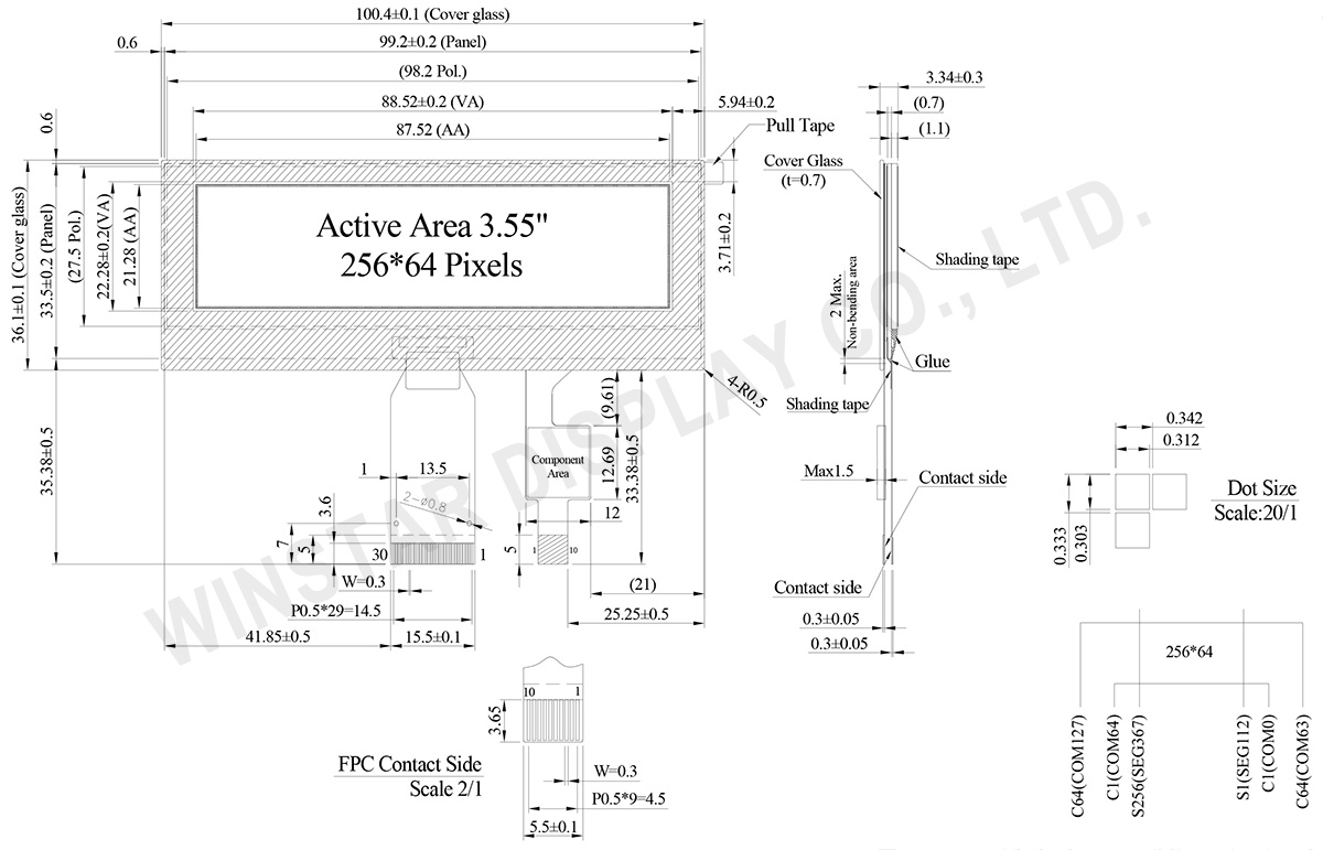
WEO025664D-CTP 為一款 3.55 吋 COG OLED 顯示模組,整合 電容式觸控面板,解析度為 256x64 dots。模組採用 SSD1322 控制 IC,支援 6800/8080 8-bit 並列介面與 3-/4-line SPI,邏輯電壓為 3.3V,顯示驅動電壓為 16V,採用 1/64 duty 驅動方式,支援 4-bit 灰階顯示。
內建 電容式觸控面板(CTP)採用 FT6336U 控制器,支援 I2C 介面與單點觸控輸入。COG(Chip-on-Glass)結構可實現更精簡的模組設計,適用於空間受限的應用環境。
操作溫度範圍為 -20°C 至 +70°C,儲存溫度範圍為 -30°C 至 +80°C。此 3.55 吋 OLED 模組適用於智慧家電、工業控制、醫療設備及通訊裝置等應用。
| 項目 | 尺寸 | 單位 |
|---|---|---|
| 點陣 | 256 × 64 Dots | - |
| 模組尺寸 | 100.4 × 36.1 × 3.34 | mm |
| 有效區域 | 87.52 × 21.28 | mm |
| 點大小 | 0.312 × 0.303 | mm |
| 點間距 | 0.342 × 0.333 | mm |
| 顯示模式 | 被動矩陣 | |
| 發光顏色 | 單色 | |
| 驅動方式 | 1/64 Duty | |
| 灰階 | 4 bits | |
| OLED IC | SSD1322 | |
| OLED 介面 | 6800, 8080, SPI | |
| 尺寸(對角線) | 3.55 吋 | |
| CTP IC | FT6336U | |
| 支援手指數 | 1 | |
| CTP 介面 | I2C | |
| 表面 | 亮面 | |
| 參數 | 符號 | 最小值 | 最大值 | 單位 |
|---|---|---|---|---|
| 工作電源電壓 | VCI | -0.3 | 4 | V |
| 邏輯電源電壓 | VDD | -0.5 | 2.75 | V |
| I/O pin 供電電壓 | VDDIO | -0.5 | VCI | V |
| 顯示電源電壓 | VCC | -0.5 | 20 | V |
| 工作溫度 | TOP | -20 | +70 | °C |
| 儲存溫度 | TSTG | -30 | +80 | °C |
| 參數 | 符號 | 最小值 | 最大值 | 單位 |
|---|---|---|---|---|
| 電源電壓 | VDD | -0.3 | 3.6 | V |
| 項目 | 符號 | 條件 | 最小值 | 典型值 | 最大值 | 單位 |
|---|---|---|---|---|---|---|
| 低壓電源 | VCI | - | 3.1 | 3.3 | 3.5 | V |
| 顯示電源電壓 | VCC | - | 15.5 | 16.0 | 16.5 | V |
| 邏輯電源電壓 | VDD | - | 2.4 | - | 2.6 | V |
| I/O Pin 電源 | VDDIO | - | 1.65 | VCI | V | |
| 輸入高準位 | VIH | - | 0.8×VDDIO | - | VDDIO | V |
| 輸入低準位 | VIL | - | 0 | - | 0.2×VDDIO | V |
| 輸出高準位 | VOH | - | 0.9×VDDIO | - | VDDIO | V |
| 輸出低準位 | VOL | - | 0 | - | 0.1×VDDIO | V |
| 50%顯示畫面耗電流 | VCC =16V | - | 35 | 55 | mA | |
| 項目 | 符號 | 條件 | 最小值 | 典型值 | 最大值 | 單位 |
|---|---|---|---|---|---|---|
| 電源電壓 | VDD | 2.8 | 3.0 | 3.3 | V | |
| 輸入高準位 | VIH | 0.7×VDD | - | VDD | V | |
| 輸入低準位 | VIL | -0.3 | - | 0.3×VDD | V | |
| 輸出高準位 | VOH | IOH = -0.1mA | 0.7×VDD | - | - | V |
| 輸出低準位 | VOL | IOH = 0.1mA | - | - | 0.3×VDD | V |
| Pin Number | 符號 | I/O | 功能說明 | ||||||||||
|---|---|---|---|---|---|---|---|---|---|---|---|---|---|
| 1 | ESD_GND | P | Ground | ||||||||||
| 2 | VSS | P | Ground. | ||||||||||
| 3 | VCC | P | Power supply for panel driving voltage. This is also the most positive power voltage supply pin. |
||||||||||
| 4 | VCOMH | P | COM signal deselected voltage level. A capacitor should be connected between this pin and VSS. |
||||||||||
| 5 | VLSS | P | Analog system ground pin. | ||||||||||
| 6~13 | D7~D0 | I/O | Host Data Input/Output Bus These pins are 8-bit bi-directional data bus to be connected to the microprocessor’s data bus. When serial mode is selected, D1 will be the serial data input SDIN and D0 will be the serial clock input SCLK. |
||||||||||
| 14 | E/RD# | I | Read/Write Enable or Read This pin is MCU interface input. When interfacing to a 68XX-series microprocessor, this pin will be used as the Enable (E) signal. Read/write operation is initiated when this pin is pulled high and the CS# is pulled low. When connecting to an 80XX-microprocessor, this pin receives the Read (RD#) signal. Data read operation is initiated when this pin is pulled low and CS# is pulled low. When serial mode is selected, this pin must be connected to VSS. |
||||||||||
| 15 | R/W# | I | Read/Write Select or Write This pin is MCU interface input. When interfacing to a 68XX-series microprocessor, this pin will be used as Read/Write (R/W#) selection input. Pull this pin to “High” for read mode and pull it to “Low” for write mode. When 80XX interface mode is selected, this pin will be the Write (WR#) input. Data write operation is initiated when this pin is pulled low and the CS# is pulled low. When serial mode is selected, this pin must be connected to VSS. |
||||||||||
| 16 | BS0 | I | Communicating Protocol Select These pins are MCU interface selection input. See the following table:
(1) 0 is connected to VSS (2) 1 is connected to VDDIO |
||||||||||
| 17 | BS1 | ||||||||||||
18 |
D/C# | I | Data/Command Control This pin is Data/Command control pin connecting to the MCU. When the pin is pulled HIGH, the content at D[7:0] will be interpreted as data. When the pin is pulled LOW, the content at D[7:0] will be interpreted as command. |
||||||||||
| 19 | CS# | I | Data/Command Control This pin is the chip select input connecting to the MCU. The chip is enabled for MCU communication only when CS# is pulled LOW. |
||||||||||
| 20 | RES# | I | This pin is reset signal input. When the pin is pulled LOW, initialization of the chip is executed. Keep this pin pull HIGH during normal operation. |
||||||||||
| 21 | FR | O | This pin is No Connection pins. Nothing should be connected to this pin. This pin should be left open individually. | ||||||||||
| 22 | IREF | I | Current Reference for Brightness Adjustment This pin is segment current reference pin. A resistor should be connected between this pin and VSS. Set the current lower than 10uA. |
||||||||||
| 23 | N.C. | - | Reserved Pin The N.C. pin between function pins are reserved for compatible and flexible design. |
||||||||||
| 24 | VDDIO | P | Power Supply for I/O Pin It should be matched with the MCU interface voltage level. |
||||||||||
| 25 | VDD | P | Power Supply for Core Logic Circuit Power supply pin for core logic operation. A capacitor is required to connect between this pin and VSS |
||||||||||
| 26 | VCI | P | Power Supply for Operation VCI must always be equal to or higher than VDD and VDDIO. |
||||||||||
| 27 | VSL | P | Voltage Output Low Level for SEG Signal This is segment voltage reference pin. When external VSL is not used, this pin should be left open. When external VSL is used, this pin should connect with resistor and diode to ground. |
||||||||||
| 28 | VLSS | P | Ground of Analog Circuit These are the analog ground pins. They should be connected to VSS externally. |
||||||||||
| 29 | VCC | P | Power Supply for OLED Panel These are the most positive voltage supply pin of the chip. They must be connected to external source. |
||||||||||
| 30 | ESD GND | P | Ground |
| 1 | GND | Ground |
| 2 | VDD | Power Supply Voltage of CTP |
| 3 | INT | External interrupt to the host |
| 4 | SDA | I2C data input and output |
| 5 | SCL | I2C clock input |
| 6 | RST | External Reset, Low is active |
| 7-10 | GND | Ground. |

通過點擊「允許所有 Cookie」,代表您同意在您的設備上存儲 Cookie 以增強網站瀏覽體驗、分析網站使用情況並協助我們的行銷和網站效能優化工作。您可以在我們的隱私權政策中找到有關於此的更多資訊。