 - WEX025664B-CTP")

 - WEX025664B")
我們重視您的隱私
通過點擊「允許所有 Cookie」,代表您同意在您的設備上存儲 Cookie 以增強網站瀏覽體驗、分析網站使用情況並協助我們的行銷和網站效能優化工作。您可以在我們的隱私權政策中找到有關於此的更多資訊。

 - WEN025664B")
 - WEN025664B")
 - WEN025664B")
 - WEN025664B")
 - WEN025664B")
 - WEN025664B")
 - WEN025664B")
 - WEN025664B")
 - WEN025664B")
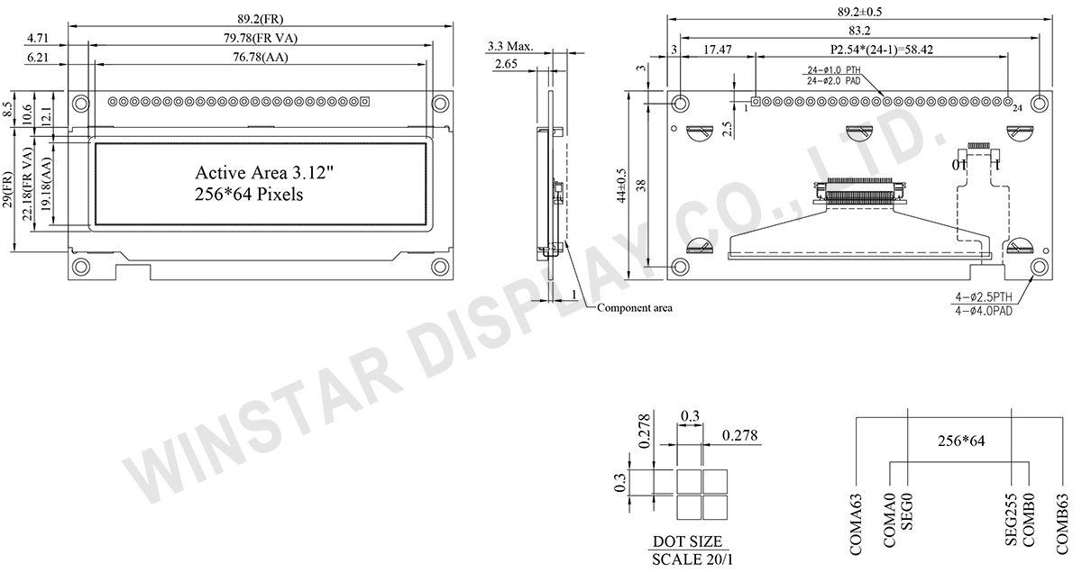
WEN025664B 為一款 3.12 吋繪圖型 COF OLED 顯示模組,解析度為 256×64 dots。此模組搭載 SSD1322 驅動 IC,支援 6800/8080 8-bit 並列介面及 3-/4-wire SPI 介面。模組外型尺寸為 89.2 × 44.0 mm,有效顯示區為 76.78 × 19.18 mm。
此模組支援 4-bit 灰階顯示,邏輯電壓為 3V,採用 1/64 duty 驅動方式。標準工作電流為 150 mA @ 3.0V VDD(50% checkerboard)。對比度為 10,000:1。操作溫度範圍為 -40°C ~ +80°C,儲存溫度範圍為 -40°C ~ +85°C。
此模組包含 PCB、金屬框及四個固定孔,可用於機構安裝。PCB 已整合 VCC 電路與介面設定。
應用範圍:智慧家電設備、醫療設備、工業控制系統,以及需使用緊湊型單色 OLED 顯示之裝置。
依機構設計與觸控需求,提供以下相關型號:
| 項目 | 尺寸 | 單位 |
|---|---|---|
| 點陣 | 256 x 64 Dots | - |
| 模組尺寸 | 89.2 × 44.0 × 3.3 Max. | mm |
| 有效區域 | 76.78 × 19.18 | mm |
| 像素大小 | 0.278 × 0.278 | mm |
| 像素間距 | 0.3×0.3 | mm |
| 顯示模式 | 被動矩陣 | |
| 發光顏色 | 單色 | |
| 驅動方式 | 1/64 Duty | |
| 灰階 | 4 bits | |
| IC | SSD1322 (COF) | |
| 介面 | 6800, 8080, SPI | |
| 尺寸 | 3.12 吋 | |
| 參數 | 符號 | 最小值 | 最大值 | 單位 |
|---|---|---|---|---|
| 顯示電源電壓 | VDD | -0.3 | 4 | V |
| 工作溫度 | TOP | -40 | 80 | °C |
| 儲存溫度 | TSTG | -40 | 85 | °C |
| 項目 | 符號 | 條件 | 最小值 | 典型值 | 最大值 | 單位 |
|---|---|---|---|---|---|---|
| 邏輯電源電壓 | VDD | - | 2.8 | 3.0 | 3.3 | V |
| 輸入高準位 | VIH | - | 0.8×VDD | - | VDD | V |
| 輸入低準位 | VIL | - | 0 | - | 0.2×VDD | V |
| 輸出高準位 | VOH | - | 0.9×VDD | - | VDD | V |
| 輸出低準位 | VOL | - | 0 | - | 0.1×VDD | V |
| 50%顯示畫面耗電流 | IDD | VCC =3V | - | 150 | 300 | mA |
| Pin Number |
符號 | I/O | 功能說明 | ||||||||||
|---|---|---|---|---|---|---|---|---|---|---|---|---|---|
| 1 | VSS | P | Ground. | ||||||||||
| 2 | VDD | P | Power Supply for Core Logic Circuit Power supply pin for core logic operation. A capacitor is required to connect between this pin and VSS |
||||||||||
| 3 | N.C. | P | Reserved Pin The N.C. pin between function pins are reserved for compatible and flexible design. |
||||||||||
| 4 | D/C# | I | Data/Command Control This pin is Data/Command control pin connecting to the MCU. When the pin is pulled HIGH, the content at D[7:0] will be interpreted as data. When the pin is pulled LOW, the content at D[7:0] will be interpreted as command. |
||||||||||
| 5 | R/W# (WR#) |
I | Read/Write Select or Write This pin is MCU interface input. When interfacing to a 68XX-series microprocessor, this pin will be used as Read/Write (R/W#) selection input. Pull this pin to “High” for read mode and pull it to “Low” for write mode. When 80XX interface mode is selected, this pin will be the Write (WR#) input. Data write operation is initiated when this pin is pulled low and the CS# is pulled low. When serial mode is selected, this pin must be connected to VSS. |
||||||||||
| 6 | E/RD# | I | Read/Write Enable or Read This pin is MCU interface input. When interfacing to a 68XX-series microprocessor, this pin will be used as the Enable (E) signal. Read/write operation is initiated when this pin is pulled high and the CS# is pulled low. When connecting to an 80XX-microprocessor, this pin receives the Read (RD#) signal. Data read operation is initiated when this pin is pulled low and CS# is pulled low. When serial mode is selected, this pin must be connected to VSS. |
||||||||||
| 7~14 | DB0 | I/O | Host Data Input/Output Bus These pins are 8-bit bi-directional data bus to be connected to the microprocessor’s data bus. When serial mode is selected, DB1 will be the serial data input SDIN and DB0 will be the serial clock input SCLK. |
||||||||||
| DB1 | |||||||||||||
| DB2 | |||||||||||||
| DB3 | |||||||||||||
| DB4 | |||||||||||||
| DB5 | |||||||||||||
| DB6 | |||||||||||||
| DB7 | |||||||||||||
| 15 | NC | P | Reserved Pin The N.C. pin between function pins are reserved for compatible and flexible design. |
||||||||||
| 16 | RES# | I | This pin is reset signal input. When the pin is pulled LOW, initialization of the chip is executed. Keep this pin pull HIGH during normal operation. |
||||||||||
| 17 | CS# | I | Data/Command Control This pin is the chip select input connecting to the MCU. The chip is enabled for MCU communication only when CS# is pulled LOW. |
||||||||||
18 |
NC | P | Reserved Pin The N.C. pin between function pins are reserved for compatible and flexible design. |
||||||||||
| 19 | BS1 | I | Communicating Protocol Select These pins are MCU interface selection input. See the following table:
(1) 0 is connected to VSS (2) 1 is connected to VDD |
||||||||||
| 20 | BS0 | ||||||||||||
| 21~24 | NC | P | Reserved Pin The N.C. pin between function pins are reserved for compatible and flexible design. |

通過點擊「允許所有 Cookie」,代表您同意在您的設備上存儲 Cookie 以增強網站瀏覽體驗、分析網站使用情況並協助我們的行銷和網站效能優化工作。您可以在我們的隱私權政策中找到有關於此的更多資訊。