 - WEX025664B-CTP")
 - WEN025664B-CTP")
 - WEX025664B")
私たちはあなたのプライバシーを大切にします
「すべてのクッキーを許可」をクリックすると、サイトのナビゲーションを向上させ、サイト使用状況を分析し、マーケティングおよびパフォーマンスの取り組みを支援するために、クッキーをデバイスに保存することに同意したことになります。この件に関する詳細情報は、ポリシーをご覧ください。プライバシーポリシー

 - WEN025664B")
 - WEN025664B")
 - WEN025664B")
 - WEN025664B")
 - WEN025664B")
 - WEN025664B")
 - WEN025664B")
 - WEN025664B")
 - WEN025664B")
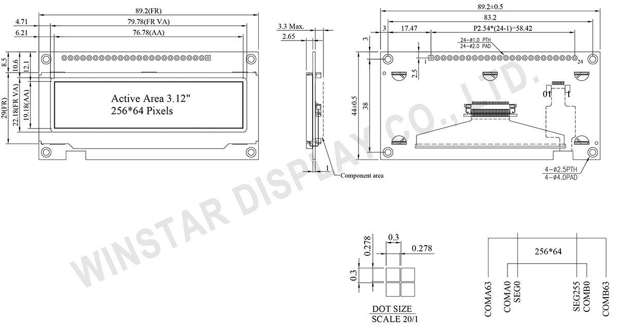
WEN025664Bは、解像度256×64ドットの3.12インチCOF構造グラフィックOLEDディスプレイモジュールです。SSD1322 ICを搭載し、6800/8080 8ビットパラレルおよび3線/4線SPIインターフェースに対応しています。外形寸法は89.2 × 44.0 mm、表示エリアは76.78 × 19.18 mmです。
本モジュールは4ビットグレースケール表示に対応し、ロジック電圧3V、1/64デューティ駆動を採用しています。標準消費電流は150 mA @ 3.0V VDD(50%チェッカーボードパターン時)です。コントラスト比は10,000:1、動作温度範囲は-40℃~+80℃、保存温度範囲は-40℃~+85℃です。
本モジュールはPCB、金属フレーム、および4つの取付穴を備え、機構組み込みに対応しています。PCBにはVCC回路およびインターフェース設定が統合されています。
主な用途:スマートホーム機器、医療機器、産業用制御機器、コンパクトなモノクロOLED表示を必要とする各種装置。
機構仕様およびタッチオプションに応じた関連モデル:
| 項目 | 仕様 | 単位 |
|---|---|---|
| ドットマトリックス | 256 x 64 Dots | - |
| モジュールサイズ | 89.2 × 44.0 × 3.3 Max. | mm |
| アクティブエリア | 76.78 × 19.18 | mm |
| ピクセルサイズ | 0.278 × 0.278 | mm |
| ピクセルピッチ | 0.3 × 0.3 | mm |
| 表示モード | パッシブマトリクス | |
| 発光色 | モノクロ | |
| 駆動方法 | 1/64 Duty | |
| グレースケール | 4 bits | |
| IC | SSD1322 (COF) | |
| インターフェイス | 6800, 8080, SPI | |
| サイズ | 3.12 インチ | |
| パラメーター | 記号 | 最小値 | 最大値 | 単位 |
|---|---|---|---|---|
| Display電源電圧 | VDD | -0.3 | 4 | V |
| 操作温度 | TOP | -40 | 80 | °C |
| 保存温度 | TSTG | -40 | 85 | °C |
| 項目 | 記号 | 条件 | 最小値 | 典型値 | 最大値 | 単位 |
|---|---|---|---|---|---|---|
| ロジック電源電圧 | VDD | - | 2.8 | 3.0 | 3.3 | V |
| 高レベル入力 | VIH | - | 0.8×VDD | - | VDD | V |
| 低レベル入力 | VIL | - | 0 | - | 0.2×VDD | V |
| 高レベル出力 | VOH | - | 0.9×VDD | - | VDD | V |
| 低レベル出力 | VOL | - | 0 | - | 0.1×VDD | V |
| 50% チェックボード動作電流 | IDD | VCC =3V | - | 150 | 300 | mA |
| Pin Number |
記号 | I/O | 説明 | ||||||||||
|---|---|---|---|---|---|---|---|---|---|---|---|---|---|
| 1 | VSS | P | Ground. | ||||||||||
| 2 | VDD | P | Power Supply for Core Logic Circuit Power supply pin for core logic operation. A capacitor is required to connect between this pin and VSS |
||||||||||
| 3 | N.C. | P | Reserved Pin The N.C. pin between function pins are reserved for compatible and flexible design. |
||||||||||
| 4 | D/C# | I | Data/Command Control This pin is Data/Command control pin connecting to the MCU. When the pin is pulled HIGH, the content at D[7:0] will be interpreted as data. When the pin is pulled LOW, the content at D[7:0] will be interpreted as command. |
||||||||||
| 5 | R/W# (WR#) |
I | Read/Write Select or Write This pin is MCU interface input. When interfacing to a 68XX-series microprocessor, this pin will be used as Read/Write (R/W#) selection input. Pull this pin to “High” for read mode and pull it to “Low” for write mode. When 80XX interface mode is selected, this pin will be the Write (WR#) input. Data write operation is initiated when this pin is pulled low and the CS# is pulled low. When serial mode is selected, this pin must be connected to VSS. |
||||||||||
| 6 | E/RD# | I | Read/Write Enable or Read This pin is MCU interface input. When interfacing to a 68XX-series microprocessor, this pin will be used as the Enable (E) signal. Read/write operation is initiated when this pin is pulled high and the CS# is pulled low. When connecting to an 80XX-microprocessor, this pin receives the Read (RD#) signal. Data read operation is initiated when this pin is pulled low and CS# is pulled low. When serial mode is selected, this pin must be connected to VSS. |
||||||||||
| 7~14 | DB0 | I/O | Host Data Input/Output Bus These pins are 8-bit bi-directional data bus to be connected to the microprocessor’s data bus. When serial mode is selected, DB1 will be the serial data input SDIN and DB0 will be the serial clock input SCLK. |
||||||||||
| DB1 | |||||||||||||
| DB2 | |||||||||||||
| DB3 | |||||||||||||
| DB4 | |||||||||||||
| DB5 | |||||||||||||
| DB6 | |||||||||||||
| DB7 | |||||||||||||
| 15 | NC | P | Reserved Pin The N.C. pin between function pins are reserved for compatible and flexible design. |
||||||||||
| 16 | RES# | I | This pin is reset signal input. When the pin is pulled LOW, initialization of the chip is executed. Keep this pin pull HIGH during normal operation. |
||||||||||
| 17 | CS# | I | Data/Command Control This pin is the chip select input connecting to the MCU. The chip is enabled for MCU communication only when CS# is pulled LOW. |
||||||||||
18 |
NC | P | Reserved Pin The N.C. pin between function pins are reserved for compatible and flexible design. |
||||||||||
| 19 | BS1 | I | Communicating Protocol Select These pins are MCU interface selection input. See the following table:
(1) 0 is connected to VSS (2) 1 is connected to VDD |
||||||||||
| 20 | BS0 | ||||||||||||
| 21~24 | NC | P | Reserved Pin The N.C. pin between function pins are reserved for compatible and flexible design. |

「すべてのクッキーを許可」をクリックすると、サイトのナビゲーションを向上させ、サイト使用状況を分析し、マーケティングおよびパフォーマンスの取り組みを支援するために、クッキーをデバイスに保存することに同意したことになります。この件に関する詳細情報は、ポリシーをご覧ください。プライバシーポリシー