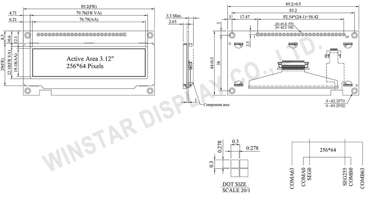
3.12" COF OLED Grafico Monocromatici 256x64 +PCB +Frame
Modello numero WEN025664B
►Tipo: grafico
►Struttura: COF+PCB+Frame
►Dimensione: 3.12 pollici
►256 x 64 a matrice di punti
►A bordo Controllore SSD1322
►Alimentatore 3V
►1/64 duty
►Interfaccia: 6800, 8080, SPI
►Colore display: Bianco / Giallo / Cielo blu / Verde
►Support Grayscale
Descrizione
Il modello WEN025664B è un display grafico OLED COF con una dimensione diagonale di 3.12 pollici e una risoluzione di 256x64 pixel. Questo modulo OLED è dotato di un IC SSD1322 e supporta interfacce SPI a 8 bit 6800/8080 e a 3/4 linee. Ha una dimensione dell'outline di 89,2 × 44,0 mm, con un'area attiva di 76,78 × 19,18 mm. Supporta anche la scala di grigi a 4 bit, con una tensione di alimentazione logica di 3V. La corrente del display al 50% sulla scheda di controllo è di 150 mA a 3,0V VDD (valore tipico), con un ciclo di lavoro di 1/64.
Il modulo ha una PCB integrata, consentendo ai clienti di utilizzare connessioni via cavo senza la necessità di sviluppare ulteriori PCB per le loro applicazioni. Inoltre, il circuito VCC integrato sulla PCB semplifica l'uso da parte dei clienti. Questa scheda PCB, dotata di quattro fori di montaggio, fornisce un metodo facile per i clienti di fissare i moduli nelle loro applicazioni. Questo modulo OLED è adatto per applicazioni smart home, dispositivi medici, controllo industriale, ecc.
Il modello WEN025664B può operare a temperature comprese tra -40°C e +80°C, con temperature di stoccaggio comprese tra -40°C e +85°C. Il modulo OLED presenta un elevato rapporto di contrasto di 10.000:1, risultando in una qualità dell'immagine migliorata, dettagli più nitidi e una migliore leggibilità, soprattutto in ambienti a bassa illuminazione.
Inoltre, i pannelli OLED con le stesse dimensioni offrono diverse alternative:- Serie WEX025664B senza telaio metallico e PCB
- Serie WEX025664B-CTP senza telaio metallico, PCB e con schermo tattile CTP
- Serie WEN025664B-CTP con telaio metallico, PCB e schermo tattile CTP
DISEGNO
Data source ref: WEN025664BWAP3N0000
SPECIFICHE TECNICHE
Funzione dei Pin di Interfaccia
Pin Number |
Simbolo | I/O | Funzione | ||||||||||
---|---|---|---|---|---|---|---|---|---|---|---|---|---|
1 | VSS | P | Ground. | ||||||||||
2 | VDD | P | Power Supply for Core Logic Circuit Power supply pin for core logic operation. A capacitor is required to connect between this pin and VSS |
||||||||||
3 | N.C. | P | Reserved Pin The N.C. pin between function pins are reserved for compatible and flexible design. |
||||||||||
4 | D/C# | I | Data/Command Control This pin is Data/Command control pin connecting to the MCU. When the pin is pulled HIGH, the content at D[7:0] will be interpreted as data. When the pin is pulled LOW, the content at D[7:0] will be interpreted as command. |
||||||||||
5 | R/W# (WR#) |
I | Read/Write Select or Write This pin is MCU interface input. When interfacing to a 68XX-series microprocessor, this pin will be used as Read/Write (R/W#) selection input. Pull this pin to “High” for read mode and pull it to “Low” for write mode. When 80XX interface mode is selected, this pin will be the Write (WR#) input. Data write operation is initiated when this pin is pulled low and the CS# is pulled low. When serial mode is selected, this pin must be connected to VSS. |
||||||||||
6 | E/RD# | I | Read/Write Enable or Read This pin is MCU interface input. When interfacing to a 68XX-series microprocessor, this pin will be used as the Enable (E) signal. Read/write operation is initiated when this pin is pulled high and the CS# is pulled low. When connecting to an 80XX-microprocessor, this pin receives the Read (RD#) signal. Data read operation is initiated when this pin is pulled low and CS# is pulled low. When serial mode is selected, this pin must be connected to VSS. |
||||||||||
7~14 | DB0 | I/O | Host Data Input/Output Bus These pins are 8-bit bi-directional data bus to be connected to the microprocessor’s data bus. When serial mode is selected, DB1 will be the serial data input SDIN and DB0 will be the serial clock input SCLK. |
||||||||||
DB1 | |||||||||||||
DB2 | |||||||||||||
DB3 | |||||||||||||
DB4 | |||||||||||||
DB5 | |||||||||||||
DB6 | |||||||||||||
DB7 | |||||||||||||
15 | NC | P | Reserved Pin The N.C. pin between function pins are reserved for compatible and flexible design. |
||||||||||
16 | RES# | I | This pin is reset signal input. When the pin is pulled LOW, initialization of the chip is executed. Keep this pin pull HIGH during normal operation. |
||||||||||
17 | CS# | I | Data/Command Control This pin is the chip select input connecting to the MCU. The chip is enabled for MCU communication only when CS# is pulled LOW. |
||||||||||
18 |
NC | P | Reserved Pin The N.C. pin between function pins are reserved for compatible and flexible design. |
||||||||||
19 | BS1 | I | Communicating Protocol Select These pins are MCU interface selection input. See the following table:
(1) 0 is connected to VSS (2) 1 is connected to VDD |
||||||||||
20 | BS0 | ||||||||||||
21~24 | NC | P | Reserved Pin The N.C. pin between function pins are reserved for compatible and flexible design. |
Dati meccanici
Articolo | Dimensioni | Unità |
---|---|---|
A matrice di punti | 256 x 64 Dots | - |
Dimensione del modulo | 89.2 × 44.0 × 3.3 Max. | mm |
Area attiva | 76.78 × 19.18 | mm |
Dimensioni del Dot | 0.278 × 0.278 | mm |
Passo del Dot | 0.3 × 0.3 | mm |
Modalità display | Matrice passiva | |
Colore display | monocromatici | |
Drive Duty | 1/64 Duty | |
Gray Scale | 4 bits | |
IC | SSD1322 (COF) | |
Interfaccia | 6800, 8080, SPI | |
Dimensione (Diagonale) | 3.12 pollici |
Valori massimi assoluti
Parameter | Simbolo | Valore Min | Valore massimo | Unità |
---|---|---|---|---|
Supply Voltage for Display | VDD | -0.3 | 4 | V |
Temperatura di lavoro | TOP | -40 | 80 | °C |
Temperatura di stock | TSTG | -40 | 85 | °C |
Caratteristiche elettriche
Articolo | Simbolo | Condizione | Valore Min | Valore tipico | Valore massimo | Unità |
---|---|---|---|---|---|---|
Supply Voltage for Display | VDD | - | 2.8 | 3.0 | 3.3 | V |
High Level Input | VIH | - | 0.8×VDD | - | VDD | V |
Low Level Input | VIL | - | 0 | - | 0.2×VDD | V |
High Level Output | VOH | - | 0.9×VDD | - | VDD | V |
Low Level Output | VOL | - | 0 | - | 0.1×VDD | V |
50% Check Board operating Current | IDD | VCC =3V | - | 150 | 300 | mA |
Search keyword: 256x64 oled, oled 256x64, 3.12 oled, 3.12" oled, 3.12 pollici oled, oled 3.12, oled 3.12"